Hest
Junior Member level 1
Hello
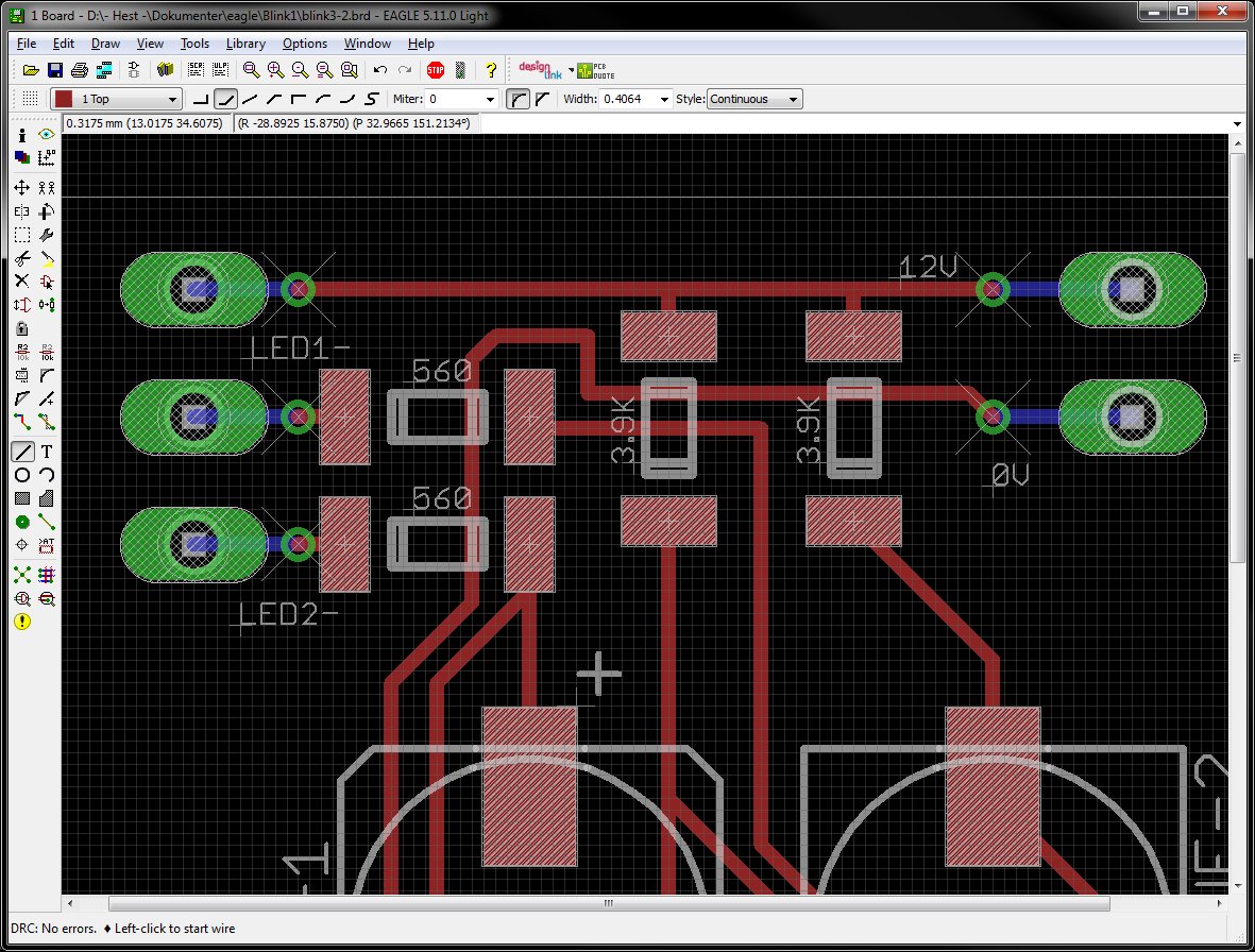
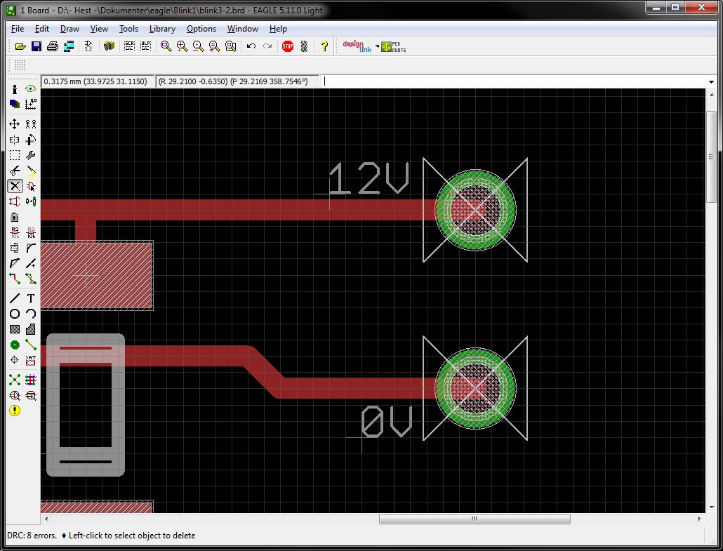
I'm now here and have only worked with Eagle for a short while, but I keep getting "Dimension" and "Drill distance" errors on by boards.
I'm trying to make a hole with a pad around, for a wire terminal. Im doing this with a via on 1mm.
When I look at the drill layer, there are no holes, so I make a hole with the drill, but no matter how large/small I do things now, I get the errors.
What am I doing wrong and why do I keep getting these errors?
How should I make a hole with a pad around?
This is how the board looks, but as I said, even if I make the holes alot smaller/larger, I still get errors.

I also added the board if anyone wants to have a look.
View attachment blink3-2.rar
I'm now here and have only worked with Eagle for a short while, but I keep getting "Dimension" and "Drill distance" errors on by boards.
I'm trying to make a hole with a pad around, for a wire terminal. Im doing this with a via on 1mm.
When I look at the drill layer, there are no holes, so I make a hole with the drill, but no matter how large/small I do things now, I get the errors.
What am I doing wrong and why do I keep getting these errors?
How should I make a hole with a pad around?
This is how the board looks, but as I said, even if I make the holes alot smaller/larger, I still get errors.
I also added the board if anyone wants to have a look.
View attachment blink3-2.rar
Last edited: