Ravinder487
Full Member level 3
- Joined
- Jul 9, 2010
- Messages
- 169
- Helped
- 0
- Reputation
- 0
- Reaction score
- 0
- Trophy points
- 1,296
- Location
- Bangalore, India
- Activity points
- 2,469
Problem with difference in driving strengths of NMOS and PMOS transistors
Hi all,
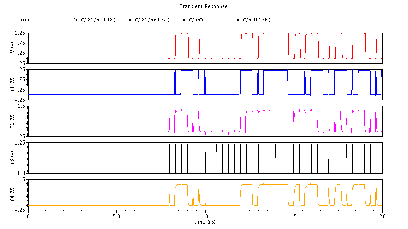
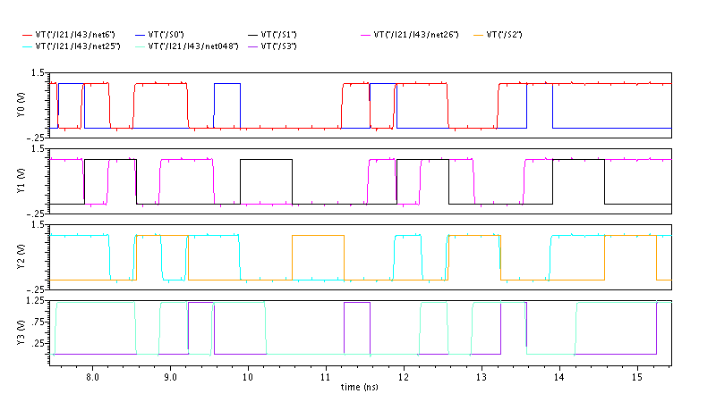
I'm designing digital circuit(consisting of MUXes and full Adder) for my ADC. At the output of my digital block I'm getting postive glitches. It seems because of difference in mobiities of NMOS and PMOS transistors. And I've verified by varying W/L of PMOS transistor.
To eliminate this I've two ideas
1) To precisely find Wp/Wn ratio for tphl=tplh for an inverter and size appropriately all the logic gates(NAND NOR etc).
2)or at the end of digital logic place a buffer-with first inverter having strong PMOS and second inverter with strong NMOS.
Which of these two method seems to be logical?
Does the same effect is seen in other logic blocks?, if so then how they will manage ?
Hi all,
I'm designing digital circuit(consisting of MUXes and full Adder) for my ADC. At the output of my digital block I'm getting postive glitches. It seems because of difference in mobiities of NMOS and PMOS transistors. And I've verified by varying W/L of PMOS transistor.
To eliminate this I've two ideas
1) To precisely find Wp/Wn ratio for tphl=tplh for an inverter and size appropriately all the logic gates(NAND NOR etc).
2)or at the end of digital logic place a buffer-with first inverter having strong PMOS and second inverter with strong NMOS.
Which of these two method seems to be logical?
Does the same effect is seen in other logic blocks?, if so then how they will manage ?
Last edited: