Continue to Site

Welcome to EDAboard.com

Welcome to our site! EDAboard.com is an international Electronics Discussion Forum focused on EDA software, circuits, schematics, books, theory, papers, asic, pld, 8051, DSP, Network, RF, Analog Design, PCB, Service Manuals... and a whole lot more! To participate you need to register. Registration is free. Click here to register now.

[SOLVED] problem with layout of resistance and capacitor

Status
Not open for further replies.

dipanjan

Member level 2
Joined
Sep 9, 2010
Messages
50
Helped
4
Reputation
8
Reaction score
4
Trophy points
1,288
Activity points
1,709
hi..
i need help using the resistors and capacitance in the umc_18_cmos library.
say i am using RNPPO_MM resistance...it has two terminals the positive and negative and a third terminal....i believe that is the body.what are the layers in its layout how to connect it i can only connect + and _ terminal am in trouble with the body
on looking at its layout i assume its a poly resistance between two layers of pdiff...but i cannot understand how i need to connect the body to the terminal...
can u tell me what the layers are and how can i connect the resistor third terminal to vdd or gnd.
i am also unsure weather for an rnppo_mm resistor i shud connect third terminal to body or gnd....
i tried putting a m1-Pdiff contact over it but it didnot work...
i keep getting an error in drc "wlnotr StampFloat "
please help tell me how to connect

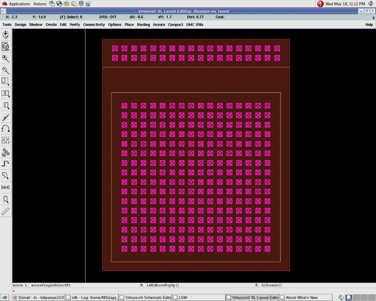
i am having similar trouble with a mimcap_mm ....it has two terminals which i can identify but what material are the contacts they appear pink in colour in layout.....can i just drag a metal wire over it and will it be connected???that will also mean i cannot roue metal wires over a cap...since the contacts are practically everyhwere....
please help i am new to using resistance and cap in layout and have no idea what to do???


please help
if u can show a screenshot of a cap (mimcap_mm) and reistance(rnppo_mm) connected between VDD and GND i will be very thankful
please in some real mess.
or show me a ckt that contains them connected in layout or a doc that might help
thank you to everyone for helping in advance
 

In order to connect the body of the resistor, you simply place it nearby a substrate connection (like the bulk connection of a transistor). You should not put the pdiff contact on top of the resistor, but somewhere next to it, dont worry too much about the distance you place it from the resistor, just make sure that it is far enough to prevent DRC errors, and obviously it should not be too far. Multiple resistors can share the same body connection. I would guess that the body should be connected to ground.

I feel your pain, I was in the same position a while back, you will pick up on IC design soon. Try reading your process documentation for a description of the available components like MOS, resistors and caps.


thanks a lot....ne insight on the connections for the capacitance?
 

thanks a lot....ne insight on the connections for the capacitance?

i keep getting in trouble with the capacitance it shows connected drc fine but lvs shows errors in connection?.

---------- Post added at 07:20 ---------- Previous post was at 06:00 ----------

In order to connect the body of the resistor, you simply place it nearby a substrate connection (like the bulk connection of a transistor). You should not put the pdiff contact on top of the resistor, but somewhere next to it, dont worry too much about the distance you place it from the resistor, just make sure that it is far enough to prevent DRC errors, and obviously it should not be too far. Multiple resistors can share the same body connection. I would guess that the body should be connected to ground.

I feel your pain, I was in the same position a while back, you will pick up on IC design soon. Try reading your process documentation for a description of the available components like MOS, resistors and caps.

i tried using pdiff m1 contact still showing stamp error float
do i need to put resistor in nwell or sumthing like that???i put resistor in the layout window which is psub layer connected the two terminals to required terminals
and put a pdiff-m1 contact just by its side and conncted to gnd....drc giving error welnotr StampErrorFloat

for cap drc no errors all connections done but lvs giving series of prblms
connected two terminals with poly for cap to metal wires..
nething i need to keep in mind while connecting a cap???
 

Hi dipanjan,

there are a few people in this forum that struggled with Assura LVS in UMC18 (apparently you have problems even in DRC), I have tried some of the devices in Calibre and they work just fine so I think is an issue with Assura; make sure you are stamping your connection using a label/pin/textDisplay in the correct layer:purpose pair (defined in Assura rules OR UMC PDK manual). I do not have Assura so I cannot help much in that area.

Contacting the bulk area sorrounding the poly resistor with m1-pdiff contact is perfectly correct; I would not go for an NWELL unless you are sure that the model supports it (it will slightly alter resistance).

I have never tried the mimcaps but I am guessing it is a similar issue.


for the resistance i guess its not required to have the pdiff-m1 touching the body or nething as long as it is close this should work.....can u show a screenshot of connection in umc 180 tech ......even if the pdiff-m1 touches the body of the resistor the error wont go ...
are u suggesting i try using calibre???
 

Nobody said the m1-pdiff contact should touch the poly resistor it should be in the bulk surrounding the poly not touching poly.

Anyway I had look at the PDK, PDIFF only works for RNNPO_MM but RNPPO_MM is set in an NWELL so to contact its well you need to use a M1-NWEL contact or an M1-NDIF in an NWELL touching the resistor NWEL shape
 

What exactly is the error saying? Did you try using an NDIFF contact instead of a PDIFF contact? The contact should NOT touch the body of the resistor, it should only be nearby. The purpose of a substrate contact (NDIFF/PDIFF) is simply to bias the substrate in the region where the resistor is placed to the desired voltage.
 

Nobody said the m1-pdiff contact should touch the poly resistor it should be in the bulk surrounding the poly not touching poly.

Anyway I had look at the PDK, PDIFF only works for RNNPO_MM but RNPPO_MM is set in an NWELL so to contact its well you need to use a M1-NWEL contact or an M1-NDIF in an NWELL touching the resistor NWEL shape


definately not the poly resistance....i meant the body of course......u say the resistance is set in Nwell but i can definately see a pdiff layer around the poly.......do u mean i have to put a nwell around it???or is there a nwell already

thank you any way
by the way can you put up the PDK document where you had a look at the sayers and connection would be great help if u dont mind
 

First of all asking for confidential document is not appropriate, second I did not find this in a document I simply tried and place a device and LVS it

body of a resistor is not a well defined proposition. Anyway RNPPO is a p-implanted poly resistor in NWELL so you need to contact the NWELL to access the central electrode represented in your symbol, in the same way you contact the NWELL when you place a PMOS
 
What exactly is the error saying? Did you try using an NDIFF contact instead of a PDIFF contact? The contact should NOT touch the body of the resistor, it should only be nearby. The purpose of a substrate contact (NDIFF/PDIFF) is simply to bias the substrate in the region where the resistor is placed to the desired voltage.

yes i tried moving the contact closer to the body .......but to no avail.......

can you tell me about the layers RNPPO_MM transistor...
by the way i am placing the resistor in a psub....for the body to be nwell i believe i would have to place a nwell around it or will it suffice to just place a m1-ndiff or m1-nwell close to the resistor body???
 

dgnani, I think it might be necessary to explain the terminology and methods a bit more clearly, since dipanjan seems to be very new to layout design. dipanjan, you should ask your company/university for your process documentation, which explains the layers and properties of each component in your technology library very clearly.

---------- Post added at 08:32 ---------- Previous post was at 08:25 ----------

dipanjan, when you place the resistor inside the NWELL, you need to bias the substrate within the nwell with the use of an NDIFF substrate contact, which must also be placed somewhere within the NWELL
 

First of all asking for confidential document is not appropriate, second I did not find this in a document I simply tried and place a device and LVS it

body of a resistor is not a well defined proposition. Anyway RNPPO is a p-implanted poly resistor in NWELL so you need to contact the NWELL to access the central electrode represented in your symbol, in the same way you contact the NWELL when you place a PMOS

i am sorry.....didnt mean it that way...
let me put it in anather way

if i am using umc with license i shud have the documents too....if u can point me where to look ...like i have a set of docs....if u can let me kno where to look it will be helpful
i am sorry for having made that inappropriate req.
sorry

thanks a lot anyway....after our conversation and having tried all three contacts (nwell-m1 ndiff-m1 and pdiff m1)
i tried placing a nwell around it
i guess since the region where i put the resistor is psub just putting a contact in close proximity is not working.
thanks a lot for your help

now the only problem i have is how to connect the capacitor...if u can please have a look at the MIMCAPS_MM in the umc_180 library ....if u may it will be really helpfull

---------- Post added at 12:47 ---------- Previous post was at 12:38 ----------

dgnani, I think it might be necessary to explain the terminology and methods a bit more clearly, since dipanjan seems to be very new to layout design. dipanjan, you should ask your company/university for your process documentation, which explains the layers and properties of each component in your technology library very clearly.

---------- Post added at 08:32 ---------- Previous post was at 08:25 ----------

dipanjan, when you place the resistor inside the NWELL, you need to bias the substrate within the nwell with the use of an NDIFF substrate contact, which must also be placed somewhere within the NWELL


i put the resistance within a nwell and used a nwell m1 contact within it and the error is gone......can u tell me what difference may occur if i use a nwell-m1 instead of ndiff-m1
i am actually confused withh the two...
ndiff shud be the layer over which poly passes to create a transistor....body shud be a simple nwell...am i right??
some where there is mention in the thread that putting the resistance in the nwell changes the resistance....
wud it happen for RNPPO_MM or were u refering to RNNPO_MM as there seems to be diff among the two in structure....

also will the performance change if i ground the body intead of vdd or vice versa and are there any norms as to where to connect the body...

sorry for so many questions
thank you


any help with the capacitance?
 
If Im correct, nwell-m1 is the same as ndiff-m1 with the addition of an nwell layer, so you can use either, within the nwell. NDIFF actually has many uses, using it as an NMOS transistor is only one. NDIFF is used as the substrate contact in an nwell, whereas PDIFF is used as the substrate contact outside of the NWELL. Yes, it does make a difference where you connect the substrate contact, usually, substrate contacts within the NWELL (NDIFF) are connected to VDD, and substrate contacts outside of the NWELL (PDIFF) are connected to GND. The capacitance should be the same procedure, you just have to figure out whether it should be inside or outside of the nwell, and then choose the appropriate substrate contact and potential.
 

If Im correct, nwell-m1 is the same as ndiff-m1 with the addition of an nwell layer, so you can use either, within the nwell. NDIFF actually has many uses, using it as an NMOS transistor is only one. NDIFF is used as the substrate contact in an nwell, whereas PDIFF is used as the substrate contact outside of the NWELL. Yes, it does make a difference where you connect the substrate contact, usually, substrate contacts within the NWELL (NDIFF) are connected to VDD, and substrate contacts outside of the NWELL (PDIFF) are connected to GND. The capacitance should be the same procedure, you just have to figure out whether it should be inside or outside of the nwell, and then choose the appropriate substrate contact and potential.

thank you ....so if the substrate of a resistance is the NWELL it should be connected to the vdd as per the above explanation....am i correct??
though in schematic connecting it to vdd or grnd doesnot cause any difference in performance i assume doing it in layout and working with extratcted values should....i will check that out in simulation.

as per the capacitance in the Umc_18_cmos it is a two terminal device so i guess there would be no effect related to the body...

my problem is i cannot recognise the contacts on the body/surface of the two transistor plates and hence dont know which material to use to connect the capacitance to the nodes it need to be connected to.
i tried with poly and this got me through DRC but the LVS error suggests the connection was wrong as all nodes connected to the CAP are showing mismatch.
 
Yes you are correct! Eventhough it has no effect in schematic, it will cause problems in layout. Lets say you have both a resistor and a PMOS in the same NWELL, if you connect the substrate contact of the resistor to GND , and the substrate contact of the PMOS to VDD, a short-circuit will be caused between VDD and GND, because of the path created through the substrate. Therefore, all of the substrate contacts within an NWELL must be connected to the same potential. How many metal contacts do the capacitor have?
 
Yes you are correct! Eventhough it has no effect in schematic, it will cause problems in layout. Lets say you have both a resistor and a PMOS in the same NWELL, if you connect the substrate contact of the resistor to GND , and the substrate contact of the PMOS to VDD, a short-circuit will be caused between VDD and GND, because of the path created through the substrate. Therefore, all of the substrate contacts within an NWELL must be connected to the same potential. How many metal contacts do the capacitor have?

yes but then i can always create two nwell for two substrates in different potential and avoid shorts...

what i wanna ask is ....since i am not very sure how these poly res function.......i can understand that the poly is a material and a long strip of it will generate a resistance.
but how is the body helping or used to make a resistor?? what is its use??

also either you or dgnani mentioned putting a nwell around a reistance may vary its resistance!!! can u suggest some reading or explain how the substrate is affecting the resistance


like in pmos the substrate potential affects the formation of channel and hence performance ...does the substrate potential vary the performance of a resistor??

---------- Post added at 15:11 ---------- Previous post was at 15:02 ----------

AS FOR THE CAPACITANCE::

i am using a mimcap_mm and it just doesnt seem to have metal contacts????i have tried connecting it with poly also......

i am attaching a screenshot of the cap... if u hav ne idea please do let me know i tried metal....and ploy though poly is giving no drc error the connections are not complete with metal drc errors are there

52_1305797864.jpg


---------- Post added at 15:12 ---------- Previous post was at 15:11 ----------

have checked all metal_* contacts ....those pink contacts match none :(
 
Yes you can if you really have to, but usually we throw all NWELLS into one in order to save area.. As I said earlier, the body provides the substrate with a potential, which is necessary for the diff to function properly, you can read into semiconductor physics if you want to learn more about this. Different doping of the diff (P/N) causes different properties. It is possible, since the substrate potential influences the density of carriers in the substrate, and thus the resistivity of the path.

---------- Post added at 11:47 ---------- Previous post was at 11:44 ----------

I am not sure, but it seems like the top group of VIAs (pink crossed squares) connect the poly to one metal contact, and the bottom group to the other metal contact. It is probably METAL 1.
 
i found those contacts to be via5.....
as u say will it connect to metal 1 i tried the connections are not working????

---------- Post added at 15:36 ---------- Previous post was at 15:36 ----------

i found those contacts to be via5.....
as u say will it connect to metal 1 i tried the connections are not working????

sorry its vi5....say now its vi 5 how do i connect it to say poly or metal??

---------- Post added at 15:43 ---------- Previous post was at 15:36 ----------

vias are usually used in contacts can u let me know in which documents to look to find out what two layers VI5 will connect (i am assuming VI5 is a via)

also can you let me know will ne documents let me know how to connect these instances and how they perform.thn i can ask the vendor to provide us with them!!!
 
Status
Not open for further replies.

Part and Inventory Search

Welcome to EDABoard.com

Sponsor

Back
Top