teep
Newbie level 3
Hi,
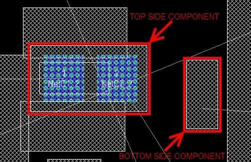
I am running Altium Designer Summer 09 and have been pulling my hair out trying to figure out how to display the cross-hatched area displaying the component boundary on the same layer as the component itself. I'm not sure how well that describes my question, so attached is an image of the problem.
In the picture, the white rectangles with cross-hatching show individual component boundaries (not sure what else to call this). I am only showing the Top Layer in this picture. As you can see, there is only one component shown that is on the top side. All the other components in this picture are located on the bottom side. However, these component boundaries are all showing up on the top side, so it looks like there is interference between the components.
I would like to be able to show these areas on the same layer as the component itself, but nothing I've tried has worked. Does anyone have any suggestions?
If what I would like to do is not possible, does anyone know if there is a way to turn off these geometries?
Thanks and if my question is not clear please let me know.