xeratule
Member level 4
- Joined
- Apr 4, 2009
- Messages
- 69
- Helped
- 1
- Reputation
- 2
- Reaction score
- 1
- Trophy points
- 1,288
- Location
- Istanbul / TURKIYE
- Activity points
- 1,975
Hi all,
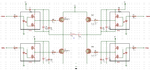
I am designing a 25khz pwm triggered full bridge circuit to drive inductive load. Please see the attached circuit. High power IGBT's are all N channel and high side IGBT's utilize from the bootstrap circuit. The pwm signals are amplified and isolated from the control circuit by the optocouplers (optocoupler outputs are CMOS). Although the circuit operates well, at high power levels one or more of the optocouplers (usually ones from high side) get destroyed.
I can't control the high frequency transients at pwm pulse edges at both positive and negative polarities. When the VCC (high power) supply voltage increases transients also gets higher. In order to protect optocoupler outputs I tried to use both varistors and TVS diodes between optocoupler supply and references.
Do you think the transients destroy the optocouplers? Is there some way to suppress those transients? Maybe my TVS diodes aren't fast enough?
I welcome those all helps. Thanks in advance.
Erhan