bobsun
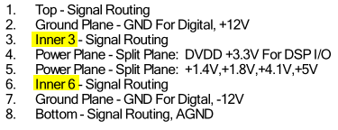
Full Member level 2
Hello,
I would like to ask a question on stripline trace.
I was reading Stripline - Wikipedia, the free encyclopedia and noted in section "Description", the articled said
What does "shorted together" mean? As far as I know, internal stripline signals are sandwiched by adjacent power planes (GND or different power), and there is nothing like "shorting". How can power and GND planes be shorted together, which incurs large burning current? Is the expression wrong here?
And what does this "row of vias running parallel to the strip" mean?
Thanks,
Bob
---------- Post added at 17:40 ---------- Previous post was at 17:27 ----------
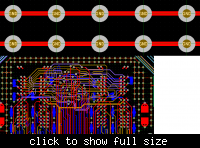
And in a DDR2 routing example as shown in the attached picture, I noticed a ribbon-like band of vias connected to GND, which are in turn connected by microstrip (NOT stripline) tracks surrounding the DDR2. They are more clearly shown in the image than the verbal description here.
What is the purpose of this GND via band? Does it have anything to do with the "shorting two ground planes" concept and the "a row of vias running parallel to the strip on each side" treatment?
Bob
I would like to ask a question on stripline trace.
I was reading Stripline - Wikipedia, the free encyclopedia and noted in section "Description", the articled said
To prevent the propagation of unwanted modes, the two ground planes must be shorted together. This is commonly achieved by a row of vias running parallel to the strip on each side.
What does "shorted together" mean? As far as I know, internal stripline signals are sandwiched by adjacent power planes (GND or different power), and there is nothing like "shorting". How can power and GND planes be shorted together, which incurs large burning current? Is the expression wrong here?
And what does this "row of vias running parallel to the strip" mean?
Thanks,
Bob
---------- Post added at 17:40 ---------- Previous post was at 17:27 ----------
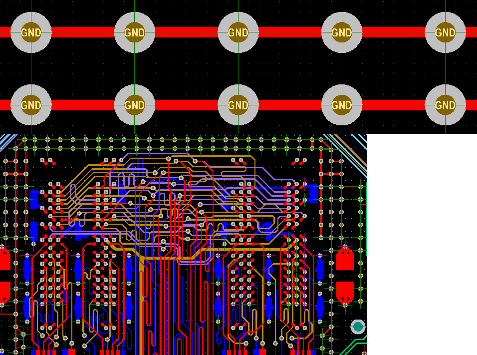
And in a DDR2 routing example as shown in the attached picture, I noticed a ribbon-like band of vias connected to GND, which are in turn connected by microstrip (NOT stripline) tracks surrounding the DDR2. They are more clearly shown in the image than the verbal description here.
What is the purpose of this GND via band? Does it have anything to do with the "shorting two ground planes" concept and the "a row of vias running parallel to the strip on each side" treatment?
Bob