Deepon
Member level 1
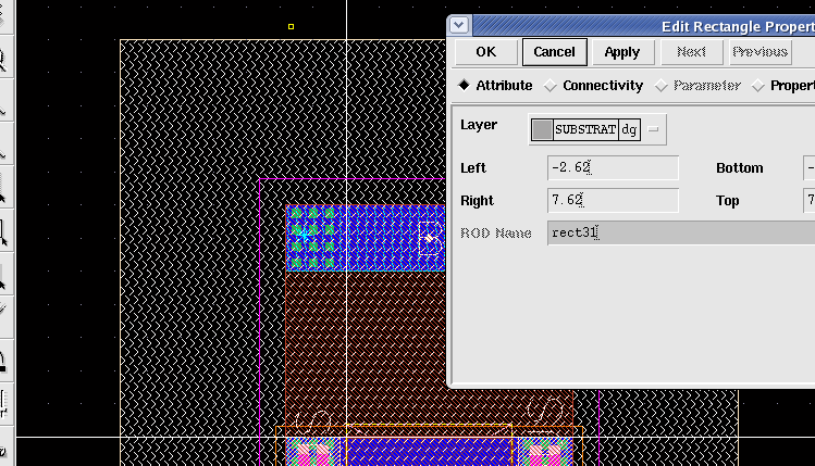
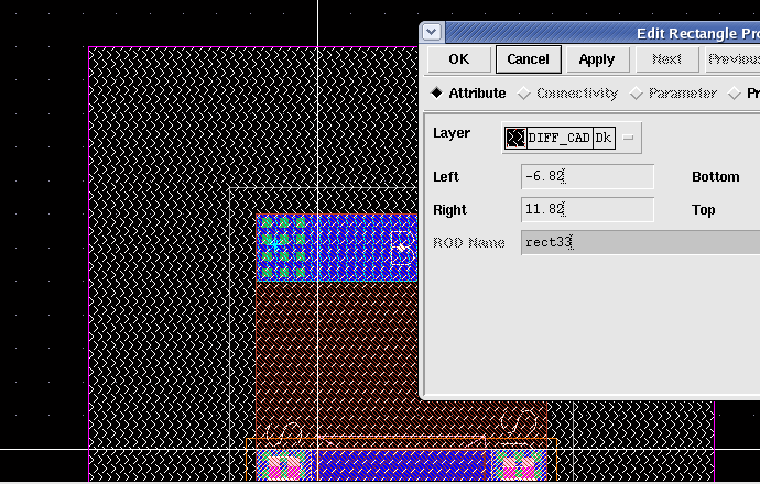
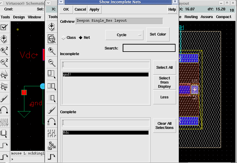
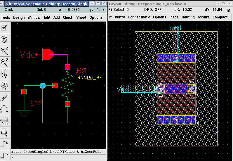
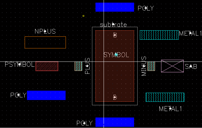
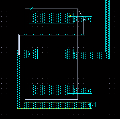
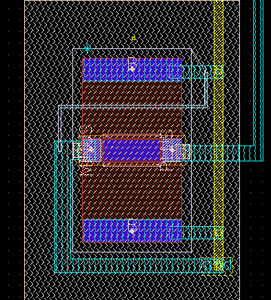
I am facing a problem while doing a simple layout of two RNNPO_RF resistors. It is showing 'gnd' in incomplete nets. I don't know how to connect the ground to the particular substrate of this resistor as it is showing in the images:
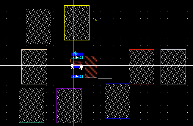
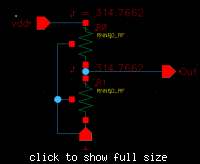
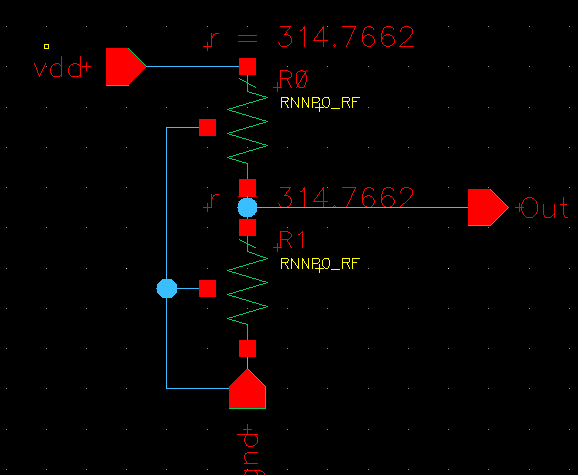
The Circuit:
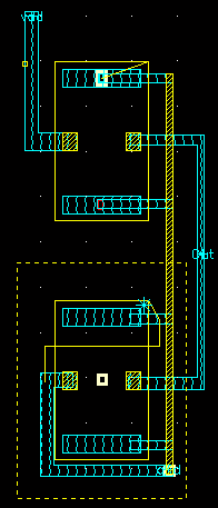
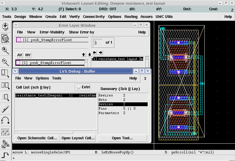
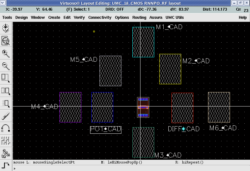
The full layout:
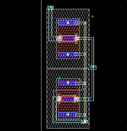
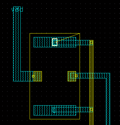
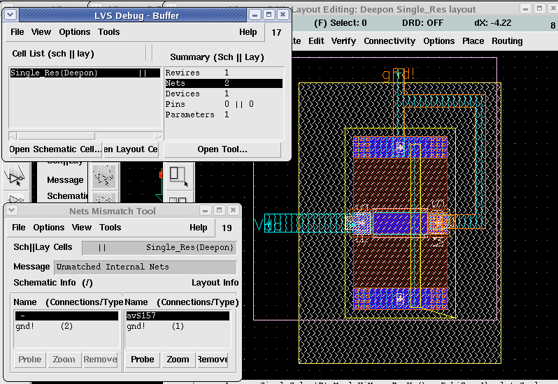
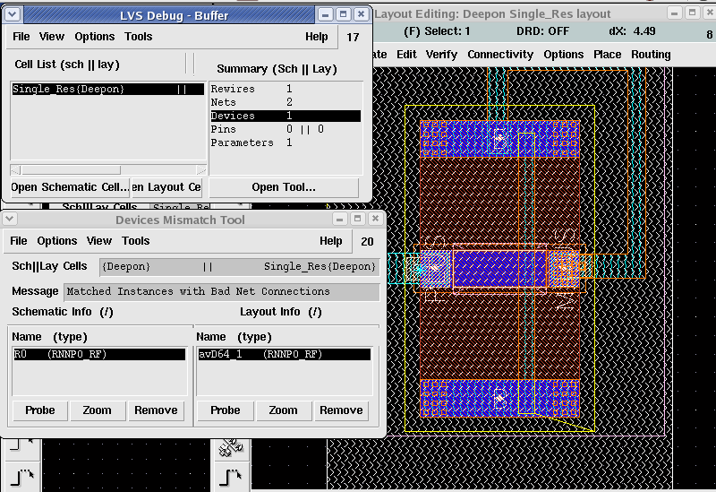
showing the incomplete nets:
How do I connect the incomplete net...
The Circuit:
The full layout:
showing the incomplete nets:
How do I connect the incomplete net...