Continue to Site

Welcome to EDAboard.com

Welcome to our site! EDAboard.com is an international Electronics Discussion Forum focused on EDA software, circuits, schematics, books, theory, papers, asic, pld, 8051, DSP, Network, RF, Analog Design, PCB, Service Manuals... and a whole lot more! To participate you need to register. Registration is free. Click here to register now.

[SOLVED] Mistake in soldermask design: Bare grounding

Status
Not open for further replies.

miskol

Member level 4
Joined
Nov 6, 2008
Messages
75
Helped
6
Reputation
12
Reaction score
6
Trophy points
1,288
Activity points
1,814
Hi,

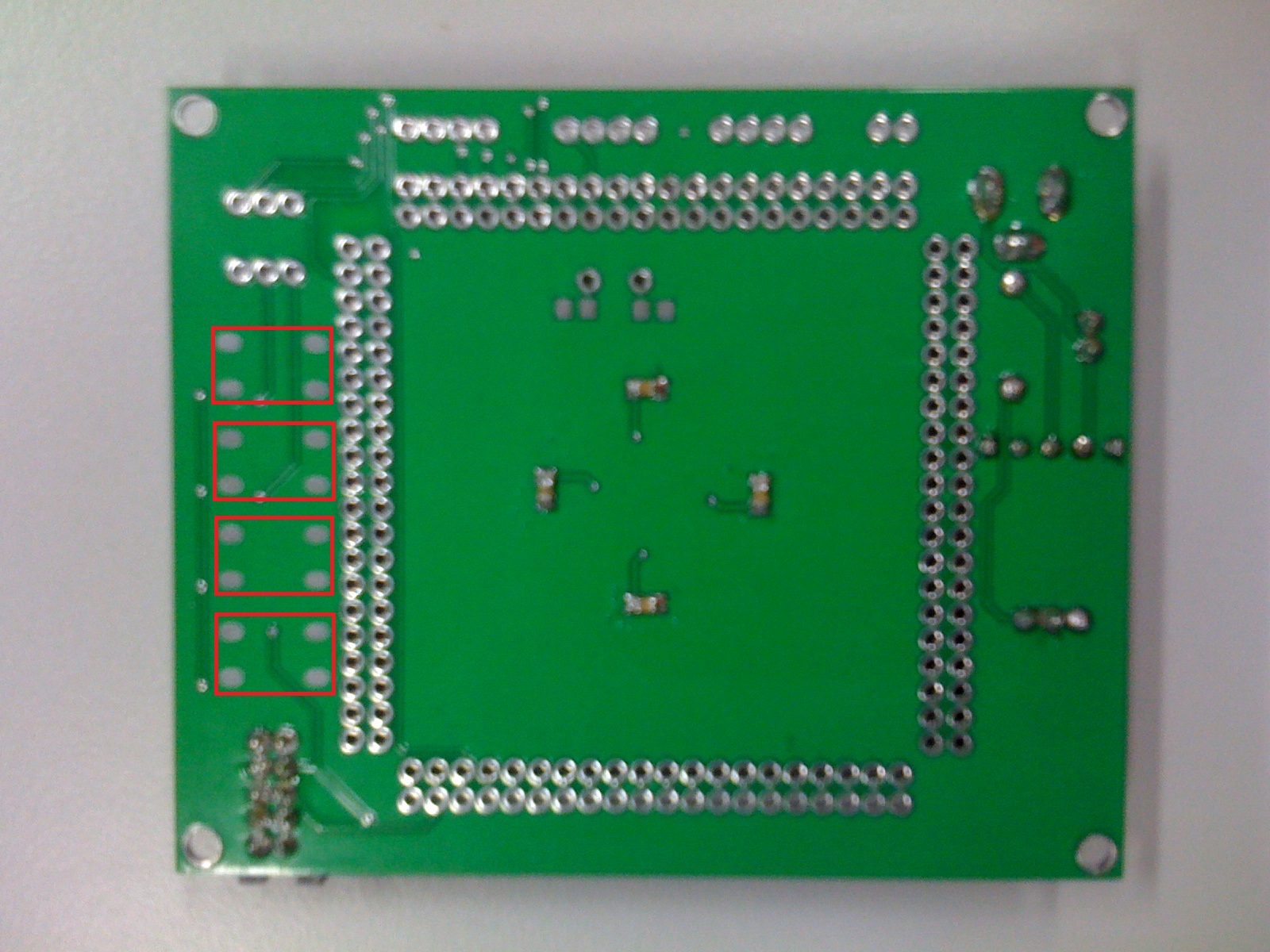
i've made a mistake in the soldermask design. as shown in the picture, the pads for the SMT tactile switch on the top layer is by mistake also made available for the bottom layer.

1) my question, is there gonna be any problem? in term of high-speed circuitry, is there any significant effect?

2) is there any easy way to repair is? can i ask the Board House for a repair?

3) any other suggestion on what should i do?

Thank you.


Just spray over it with a can of Lacquer.

If you have lots of these you can always ask the fab house to paint a little resist on them.
Or if they are going to make more then ask them to remove them from the artwork.

However - do they really cause a problem that canot be resolved in the next revision? (there is always more lol).
 

I don't see a problem either. There should be no effect in terms of high-speed circuitry.

Tape, nail polish, mylar could fix it.

I would wait for the next rev to fix it as well.
 

It shouldn't be a problem as long as it is not in contact with any traces or pads.

Apply RTV on the pads if necessary. Probably u can wait for the next revision!

All the best!
 

Looks like you got lucky and they missed all the copper signals, just the bottom layer pour/plane. If there is the potential of something pressing against the board in those spots and shorting to that plane, then some dielectric (kapton tape would do) to cover. But seeing as you have non-zero height thru-hole parts nearby, unless your chassis was rises up right at that spot you will have clearance.

Also, resolution is low, but clean that flux off the connector in the bottom left. :)
 

Status
Not open for further replies.

Part and Inventory Search

Welcome to EDABoard.com

Sponsor

Back
Top