Continue to Site

Welcome to EDAboard.com

Welcome to our site! EDAboard.com is an international Electronics Discussion Forum focused on EDA software, circuits, schematics, books, theory, papers, asic, pld, 8051, DSP, Network, RF, Analog Design, PCB, Service Manuals... and a whole lot more! To participate you need to register. Registration is free. Click here to register now.

Questions about using ARES

Status
Not open for further replies.

doandok

Newbie level 3
Joined
Mar 5, 2011
Messages
3
Helped
0
Reputation
0
Reaction score
0
Trophy points
1,281
Activity points
1,297
hello engineers, i want to know how to determine the size of PCB Board in ARES it's edges, a nother question if there is two tracks cut each other what i do in this case to remove one of them and place it with a bridge???
 

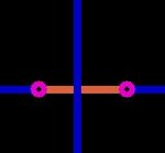
You have already found mu post in another thread but let me also add a picture of what i mean.

ARES_cross.jpg

In the above picture you can see the bottom layer (blue) tracks and i use the layer inner1 (orange) to represent the jumper so that the connection is detected in the connectivity check.

When you export to PCB you have to unchecked the inner layer because you don't want it printed as a track, you will only print the top/bottom track.

About the size of a PCB you can use a horizontal and vertical "ruler" which is used to measure a distance (dimension mode icon over the rotate clockwise).

You can also draw a 2D graphic box but the height amd width are only shown in the bottom status bar while you are creating it, you can't see them after that.

You can also draw the box aroung the PCB and then also add the "rulers" to both sides

Alex
 
thanks for ur reply but i want to know how to draw the 2-D box and i want to know how to distinguish the holes which i 'll make a jumper on them from the other holes especially if the circuit contains many jumpers, thanks again
 

You can use an export (or print) and check only the inner1 layer and top/bottom silk but uncheck the top/bottom layer,
that way only the jumpers will be shown and the component silk.

The 2D box is the blue square in the left side icons, under the red pads.

Alex
 

Status
Not open for further replies.

Part and Inventory Search

Welcome to EDABoard.com

Sponsor

Back
Top