Ravinder487
Full Member level 3
- Joined
- Jul 9, 2010
- Messages
- 169
- Helped
- 0
- Reputation
- 0
- Reaction score
- 0
- Trophy points
- 1,296
- Location
- Bangalore, India
- Activity points
- 2,469
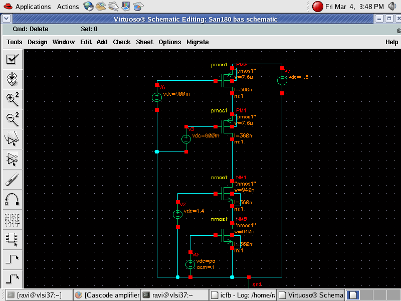
Hi all,
I'm trying to design Cascode amplifier(with cascode current mirror as load) in 180nm technology(@vdd=1.8 ) with following specifications
voltage gain 50V/V output swing .6v and ouput impedance of 4Mohm.
I first started by assuming overdrive voltages of all the transistors are same,so with this assumption my Vod is coming to be .3V.With Vod=.3 and Vth=500m my VGS<800m.From my slewrate and powerdissipation constraints I have fixed my bias current.With bias current and VGS(800m) in hand I've calculated the W/L of all the transistors.
With L=180nm I'm getting a gain of 10.2.So I doubled L(and also W in proportion) of all the transistors but my gain isn't getting 4times!! (WHY??)
And with this method I'm getting very low input swing(around 70mV).
How to find ouput resistance of Cascode amplifier?