Continue to Site

Welcome to EDAboard.com

Welcome to our site! EDAboard.com is an international Electronics Discussion Forum focused on EDA software, circuits, schematics, books, theory, papers, asic, pld, 8051, DSP, Network, RF, Analog Design, PCB, Service Manuals... and a whole lot more! To participate you need to register. Registration is free. Click here to register now.

Sigma delta ADC question ( somebody help me please ) !

Status
Not open for further replies.

egyeng1

Newbie level 6
Joined
Jun 27, 2010
Messages
12
Helped
0
Reputation
0
Reaction score
0
Trophy points
1,281
Location
EGYPT
Activity points
1,379
hi all,
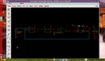
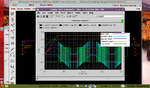
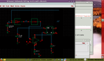
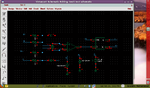
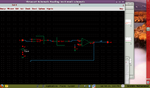
I'm doing a graduation project about Delta-Sigma ADC i started with the system level design using schreier tool and his book " Understanding Delta-Sigma Data converters" . I'm now determined with my OSR , Order , BW and DR . Now i'm asked to do a modelling for thoses parameters using Verilog.A blocks in Cadence.
My question:
1) How can i model ,as a 1st step, a 1st order delta-sigma adc ?
2) does it differ in the modelling to be continuous or discrete structures ?
3) how can i involve the specs i got (eg OSR) within the blocks ? please help me
 

You should select a simple functional diagram from the textbook and try to implement it in Verilog A. I'm not working with this simulator, but I assume, it can represent DT and CT sigma delta circuits as well. The difference is only in the integrator implementation and won't be large for the 1st order. The SD parameters will go to the structure definition of your design. OSR is implemented as decimation factor of the decimation filter processing the single bit output data stream of the SD modulator.
 

You should select a simple functional diagram from the textbook and try to implement it in Verilog A. I'm not working with this simulator, but I assume, it can represent DT and CT sigma delta circuits as well. The difference is only in the integrator implementation and won't be large for the 1st order. The SD parameters will go to the structure definition of your design. OSR is implemented as decimation factor of the decimation filter processing the single bit output data stream of the SD modulator.
If i put just blocks like subtractor , integrator , Comparator and D-ff for example where can i involve the sampling frequency in the modulator to see how it affects the modulator output ?
please have a look at the attachment to see what i've tried till now
 

Attachments

  • Screenshot-1.png
    Screenshot-1.png
    157.7 KB · Views: 155
  • Screenshot-2.png
    Screenshot-2.png
    147.7 KB · Views: 137
  • Screenshot.png
    Screenshot.png
    145.4 KB · Views: 130

The clk frequency to the DFFs is representing your SD sample clock.

Please consider, that I'm not actually involved in SD design. I have Schreier and some other literature and hopefully understood the principle. But that's it. I won't detect a design fault in your diagrams at first sight. Other edaboard members may be more involved with SD design.

Thank you my friend anyway , i did put the clk of the d_ff as the sampling frequency but the model itself still not working don't know why ? i hope somebody could just have a look on my blocks i put there and tell me what shall i do to get it working ...... thanks in advance
 

Hi egyeng,

You might find this schematic helpful. It is a CT topology.

It is a second order design, and was originally set up by a James Lawson in the UK. It is not in verilog but in LTSpice (LTSpice - can be downloaded from Linear Technology - Design Simulation and Device Models should you be interested).

It appears to work in LTSpice although I have not yet had been around to verify the output.

Best regards,

Jesper

P.S.: Will you be able to setup topology, calculate (i.e. also have time to, be interested in etc.) a third-order DS A/D? I can pay you to do so - although not huge amounts ...
 

Attachments

  • second-order-Delta-sigma.pdf
    14.2 KB · Views: 162
Last edited:

Hi egyeng,

You might find this schematic helpful. It is a CT topology.

It is a second order design, and was originally set up by a James Lawson in the UK. It is not in verilog but in LTSpice (LTSpice - can be downloaded from Linear Technology - Design Simulation and Device Models should you be interested).

It appears to work in LTSpice although I have not yet had been around to verify the output.

Best regards,

Jesper

P.S.: Will you be able to setup topology, calculate (i.e. also have time to, be interested in etc.) a third-order DS A/D? I can pay you to do so - although not huge amounts ...

First thank you sir for the pdf you attached here it really helps and ensures what i was doing , and concerning your request i'm actually in my graduation year and i'm doing a graduation project at the moment and have no time for now sorry sir i would really help you even without money( I'm not looking for money ) at least for now ;) ( Lol: ) . may be after the graduation project i will help you for sure .

I'm still waiting for more experts like all of you to give their opinions and bright ideas for this issue of discussion thanks in advance .... :)

---------- Post added at 16:20 ---------- Previous post was at 14:57 ----------

hi again friend Jesper,

- It was really a good schematic you put there do you have any other of the same kind , if so please attach them . it was really good!

regards,
Ibrahim Muhammed
 

Hi Ibrahim,

Good to hear that the schematic was of good use - kudos to James Lawson. As I myself am in a process of learning about D/S converters I do not have any more schematics but a suggestion is that you try to change the values and see what happens. Good luck with your graduation project :)

Greetings,

Jesper
 

If i put just blocks like subtractor , integrator , Comparator and D-ff for example where can i involve the sampling frequency in the modulator to see how it affects the modulator output ?
please have a look at the attachment to see what i've tried till now

Hi friend,

As i have designed 1-bit sigma-delta ADC block through simulink model, and afterwards i have designed decimation filter too.

So please express you design goal and upto how-many order you want to implement your sigma-delta modulator.

let me know ASAP to resolve the issue, with specification of your requirement.

hello gauta,
I'm so happy receiving that help from all of you , but what i want my friend is to learn and think myself my goal is not to copy ideas or to give you the specs and you give me the rest :) ... It's not like that .... I hope just to give me a clue to complete my way . Until now ,with the aid of the other friend jesper, i've done the model of the 1st order but i have a problem... how can i convert the flip-flop-out signal to analog voltage to be fed back to the integrator because i have plotted the signal at the input of the integrator but it seems different than the normal shape that we know signal doesn't follow the sine wave input for some reason

i have another question how can i get the BW of the system model ? i tried AC sweep but it didn't work :( ....lol

Sorry for the long paragraph above ...... ;) waiting for help .. and thanks in advance

Regards,
Ibrahim Muhammed
 

hey guys,
Please keep up to date with me the last thing i got is what i attach here it's a 1st order model using cadence and the output signal

there's something weird which i can't explain the signal after the integrator is not around zero but some other voltage and also after the comparator has a similar shape have a look please on the signals and even at the beginning of the signal ( after the integrator ) it's increasing for some period of time then it starts to follow the input sine wave signal , BUT the most weird thing is that it works soooooooooooo well and the input signal frequency is in the output spectrum and has a high value that means the system works well , any ideas ???
Thanks in advance

Regards,
Ibrahim Muhammed
 

Attachments

  • model_new.png
    model_new.png
    166.2 KB · Views: 143
  • all_sigs.png
    all_sigs.png
    232.6 KB · Views: 141

hey guys,
Please keep up to date with me the last thing i got is what i attach here it's a 1st order model using cadence and the output signal

there's something weird which i can't explain the signal after the integrator is not around zero but some other voltage and also after the comparator has a similar shape have a look please on the signals and even at the beginning of the signal ( after the integrator ) it's increasing for some period of time then it starts to follow the input sine wave signal , BUT the most weird thing is that it works soooooooooooo well and the input signal frequency is in the output spectrum and has a high value that means the system works well , any ideas ???
Thanks in advance

Regards,
Ibrahim Muhammed

I have verilog A code for delta sigma modulator. Every block is written in Verilog A, Its simple. I believe you are being misled.
 

Status
Not open for further replies.

Similar threads

Part and Inventory Search

Welcome to EDABoard.com

Sponsor

Back
Top