Continue to Site

Welcome to EDAboard.com

Welcome to our site! EDAboard.com is an international Electronics Discussion Forum focused on EDA software, circuits, schematics, books, theory, papers, asic, pld, 8051, DSP, Network, RF, Analog Design, PCB, Service Manuals... and a whole lot more! To participate you need to register. Registration is free. Click here to register now.

Transistor as a switch

Status
Not open for further replies.

hayowazzup

Advanced Member level 4
Joined
Oct 9, 2010
Messages
117
Helped
0
Reputation
0
Reaction score
0
Trophy points
1,296
Activity points
2,136
Hi, I'm trying to understand how transistor switch works on an oscillator,

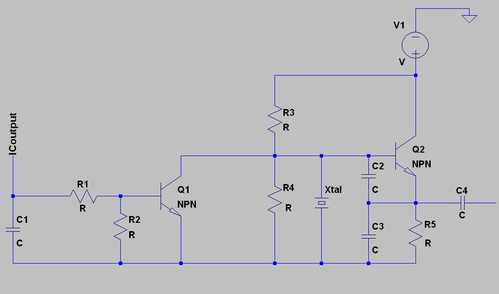
If a transistor acts as a switch, like in the diagram
trswinpn.gif

And replace RL with the oscillator crystal_oscillator.gif,
so now the collector terminal from the switch is instead connected to the base terminal of the transistor in the oscillator.

When output from the chip is 1 (ON), the transistor switch is saturated. Does the transistor switch draws most of the current from oscillator to the transistor(switch)'s emitter? which mean the oscillator won't have power to amplify. so it's considered Off.

in contrast, when the IC output is 0 (OFF) , the transistor switch is in cutoff region, there will be no current extracted from the power supply to the switch's emitter, so oscillator will have power to amplify and is considered ON.
 
Last edited:

Does the transistor switch draws most of the current from oscillator to the transistor(switch)'s emitter? which mean the oscillator won't have power to amplify. so it's considered Off.
In my understanding, the switch transistor would simply cut off the transistor bias current. But there are more simpe methods to turn the oscillator off, e.g. supplying R1 from a digital output signal.
 

hi,
so do you agree that the digital 1 switches off the oscillator whereas 0 will turn it on?

and by supplying R1 from a digital output signal,
do you mean connecting the digital output directly to base terminal of the amplifier, or the other side of R1?
so it'll work as there's clipping?

thanks
 

As I know, transistor in some crystal OSC circuit works in satuation region always. It is not a switch.
However, your circuit is confused.
 

You didn't read the question exactly. It's about a second transistor, not shown in the circuit. Somewhat unclear, in fact.
 

sorry about my question is unclear
there's two diagrams attached, one is the switch circuit, trswinpn.gif (somehow it doesn't show).
Another one is the oscillator circuit.

My question is simply about how does the switch circuit work on the oscillator (acting as the load RL)

thanks for the replies by the way.
 
Last edited:

Basically Vcc charges the crystal which begins to oscillate. R2, C1, and C3 keep the oscillation of the crystal oscillations going. R2 and R1 act as a bias for the base of the transistor which is oscillating, and the transistor is being turned on and off at the frequency of the crystal. The voltage swing goes from 0V to Vcc and back to 0V in a complete cycle. The capacitor which is connected to the emitter of the transistor is just a dc blocking capacitor keeping the dc bias voltage from entering the crystal oscillation waveform when the transistor is turning on and off rapidly.
 

@cmancuso I think you've misunderstood the OP's question, but there's been a lot of confusion on this thread.
It would help if the OP gave us one single circuit, rather than the two circuits and asking us to imagine how one of his circuits (the switch) turns the other circuit (the oscillator) on and off.

@hayowazzup
My own understanding of your question is, YES, the switch WILL turn the oscillator on and off.
But its a very poor way of doing it! Apart from the poor current paths and the DC thump when switching the oscillator on and off, it is quite unnecessary to do it this way.

If you concentrate on the oscillator circuit and ask the simple question: what is the most effective method of turning this oscillator on or off?, then I think you'll find better solutions.
If your switch is local and mechanical, you could simply disconnect one end of the crystal or break the circuit's output connection.
If your switch is remote and/or electronic, then I'd advise using your 'switch circuit' so that the collector | emitter terminals of the 'switch' are connected across the crystal (so that the 'switch' either lets it operate as an oscillator or shorts it causing it to stop oscillating.

(You could also consider letting the oscillator run continuously, and apply the 'switch' circuit to its output. This could clamp the output to ground when you want to switch the oscillator's output 'off', and leave the output unnaffected when you want the oscillator to be 'on'.
Hope this helps
 

hi, I've just drawn out the circuit. (forgot to add the ground)


@cmancuso by "the transistor is being turned on and off at the frequency of the crystal" , do you mean the transistor working as a switch, not an amplifier?

@DXNewCastle The IC output from the left side of the circuit will be an unique On OFF sequence and drives the oscillator on and off by using the 'switch'. Is there no need to have a transistor 'switch' to do this job?
 
Last edited:

Is there no need to have a transistor 'switch' to do this job?
No. E.g. by supplying the oscillator bias from the logic signal, as previously suggested. But it's easy enough to figure it out yourself, I think.
 
Agreed.
Its easier than you seem to realise to stop a simple oscillator like this from oscllating!
 

@hayowazzup:
The Transistor Q2 works as a switch with feedback to the parallel resonant circuit via C2/C3. Therefore R4 is necessary not to break the crystal. This design is called Clapp-Oscillator.
Another very popular circuit is the Pierce-Oscillator, it uses Inverters instead of transistors.

BTW: Switching On/Off the oscillator by shorting the resonant circuit with Q1 is like stopping a car by pressing the brake without the clutch.
 

when Input applied, transistor will be in saturation mode, current will take the easiest path to ground.
when input is below 0.7 Vbe transistor is in Cutt off region, and it will take the path of the load.
 

Status
Not open for further replies.

Part and Inventory Search

Welcome to EDABoard.com

Sponsor

Back
Top