Continue to Site

Welcome to EDAboard.com

Welcome to our site! EDAboard.com is an international Electronics Discussion Forum focused on EDA software, circuits, schematics, books, theory, papers, asic, pld, 8051, DSP, Network, RF, Analog Design, PCB, Service Manuals... and a whole lot more! To participate you need to register. Registration is free. Click here to register now.

Op amp Current monitor help

Status
Not open for further replies.

hithesh123

Full Member level 6
Joined
Nov 21, 2009
Messages
324
Helped
1
Reputation
2
Reaction score
1
Trophy points
1,298
Location
lax
Activity points
3,548
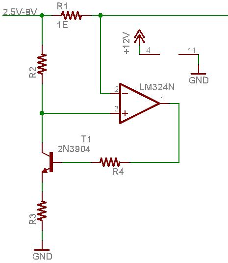
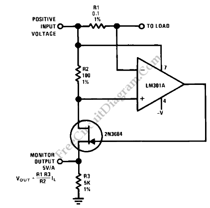
I don't understand how this opamp current monitor ckt works. I find it difficult to comprehend whenever there is an active element in the op amp feedback loop.
Can someone explain how it works and how does the offset and BJT gain affect the output.
ckt - https://obrazki.elektroda.pl/53_1296445644.jpg
 

Once feedback is working, the opamp inputs are in virtual short, and R2 current is 1/1000th that of R1 (ie IL).
R3 will have (beta+1)/beta the current of R1.
vo=I(R3)*R3=((beta+1)/1000beta)*IL*R3

Try working out the effect of offset for yourself.
 

checkmate, I don't get it.
What exactly is virtual short. Both opamp inputs are at the same potential?
what will this do to the BJT?

R3 will have (beta+1)/beta the current of R1.
Can you please explain in detail.
 

checkmate, I don't get it.
What exactly is virtual short. Both opamp inputs are at the same potential?
what will this do to the BJT?
Virtual short is one of the most basic opamp concepts. If you do not know about it, you should revisit your opamp concepts.

Can you please explain in detail.
I(R3)=I(R2)+Ib=I(R2)+(1/beta)I(R2)=((beta+b)/beta)I(R2)
Apologies about the typo previously.
 

The term "virtual short" describes the OP circuit behavior, it doesn't explain it. It's just another word for the fact, that the OP tries to zero its input differential voltage, if the feedback is setup correctly and the circuit parameters allow it.

To try an intuitive explanation, the current through R1 causes a positive voltage difference at the OP inputs. The OP acts with a positive output voltage, which increases the current source output current and reduces the OP input voltage. So you have negative feedback, as required. Because the transistor inverts the polarity of the OP output signal, the feedback goes to the positive input.
 
To try an intuitive explanation, the current through R1 causes a positive voltage difference at the OP inputs. The OP acts with a positive output voltage, which increases the current source output current and reduces the OP input voltage. So you have negative feedback, as required. Because the transistor inverts the polarity of the OP output signal, the feedback goes to the positive input.

I know virtual ground. But it's the first time I heard virtual short.

Anyway, here's what I understand -

1. Current of say, 1Amp is flowing into the load. This causes a drop of 100mV across the sense resistor.
2. Opamp senses this voltage across its input and drives its output towards the +ve rail. This will turn ON the BJT
3. Current starts flowing thru the BJT. But how much current and how to figure this out.
 

I know virtual ground. But it's the first time I heard virtual short.
I'd prefer to call it virtual short, as virtual ground is only a specific case of virtual short. Just forget virtual ground and concentrate on virtual short.

3. Current starts flowing thru the BJT. But how much current and how to figure this out.
The opamp will try its best to ensure that the BJT draws the exact current to satisfy the virtual short condition.
 
Last edited:
3. Current starts flowing thru the BJT. But how much current and how to figure this out.

As the current increases the voltage drop on R2 increases too and that lowers the opamp positive input voltage,
this reduces the difference between the 2 inputs (of the opamp) and the opamp drives the transistor base with lower voltage,
this is a very fast loop that is balanced at some point when the current flowing through R2 creates a voltage drop equal to the voltage drop of R1 so that both opamp inputs have almost the same voltage.

Alex
 
Last edited:

Great. I kinda get the idea about the opamp. Where is the negative feedback coming from?
When the BJT turns on, how much current flows thru it?
Is it according to the voltage divider rule?
1.1K in one branch and 0.1 ohm and load resistor in the other branch.
 

the opamp tries to match the voltage drop on 0.1 ohm with the voltage drop on the 100 ohm resistor,
for every ampere through the 0.1 ohm resistor you get 1mA through the 100 ohm resistor and because this current also flows through the 1K resistor you get 1K*1mA=1V output (for every amp on the load)

Alex
 
alexan_e, I got it finally. To eqalize the voltage at both its terminals, the opamp turns ON the BJT such that the required current flows until the +ve input voltage equals the -ve input voltage.
I used look at this circuit and wonder how it works, until now.
Thanks to all you guys.

---------- Post added at 17:55 ---------- Previous post was at 17:49 ----------

Guys, are there any other opamp circuits that are similar - with active elements in the feedback loop?
can you post links.
 

Guys, are there any other opamp circuits that are similar - with active elements in the feedback loop?
can you post links.

Did you hear about the phase-lead integrator? That`s a non-inverting integrator, which has an inverting circuit (ie.g. opamp inverter) in the feedback path, that is connected to the pos. input of the main opamp (inv. terminal grounded).
 

No, can you post a link to the ckt?
 

I used look at this circuit and wonder how it works, until now.
Some additional stuff to wonder: The circuit, that can be found in the LM358 datasheet, is also susceptible to latch-up. If you manage to raise the OP output voltage above the input voltage and get the base-collector junction forward biased, you possibly change the circuit operation to positive feedback and make it latch and never recover before the supply is shut down. By chance, this can already happen when powering the circuit. By placing a base series resistance, you can prevent from this accidental operation.
 
By placing a base series resistance, you can prevent from this accidental operation.

Hello FvM ,
Would this circuit have latchup problems ? The current would be in the range of 1~100mA , with a supply voltage of 2.5V ~ 8V. The LM124 would be supplied by a voltage of 12V.Any suggestions on how to size the base resistor value ?
 

Would this circuit have latchup problems ?
Yes, if you manage to foward bias the BC junction. Doesn't happen under regular conditions. R4 works mainly as current limiter when the input voltage is missing. The value isn't critical, may be 5 to 10 times R2. For R2 > R3, a compensation capacitor may be required to achieve stability.
 

For R2 > R3, a compensation capacitor may be required to achieve stability.
I think that will be a case when we want to attenuate the sensed voltage? Where would the compensation capacitor be applied ?

In topologies like this,is it possible to calibrate out the effect of offset voltage of the OpAmp using a trimmer ?

Thanks.
 

The compensation has to reduce the feedback factor to below < 1 without reducing the phase margin. An RC series circuit from transistor base to V+ would be an option. But it's simpler to adjust R1 and R2 to avoid the R2 > R3 case.

I also wonder, if you shouldn't better use the PNP variant of this circuit.

Offset compensation can be supplemented, but needs a constant (reference) voltage. I would prefer a low offset OP.
 

I also wonder, if you shouldn't better use the PNP variant of this circuit.
I would prefer a low offset OP.

FvM,
I was not able to get any PNP version of the circuit,though there is one with a n-channel MOSFET.Can you point me to any link ?
Is there any advantage of a PNP version or even the MOSFET version ?


For the PNP or PMOSFET variant of the circuit, you can refer to the design principle of commercially available current sense ICs, e.g. **broken link removed**

The main difference is, that the transistors operates in common collector configuration for the feedback path.
 

Status
Not open for further replies.

Similar threads

Part and Inventory Search

Welcome to EDABoard.com

Sponsor

Back
Top