jeetz_mail
Newbie level 6
Hi
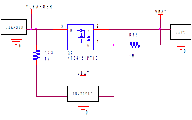
Please see the attached file for my circuit.
Circuit description:
I am trying to charge a battery through a PFET switch, Q2. When charger is connected, it pulls Vcharger high, which causes the inverter output to be low and turns Q2 ON. The problem is that when the charger is removed, Q2 switch will feed back VBAT to Vcharger, therefore, reinforcing the inverter output to be low and keeping Q2 ON forever.
Any ideas on how to solve this issue?
Thanks
Jeet