Continue to Site

Welcome to EDAboard.com

Welcome to our site! EDAboard.com is an international Electronics Discussion Forum focused on EDA software, circuits, schematics, books, theory, papers, asic, pld, 8051, DSP, Network, RF, Analog Design, PCB, Service Manuals... and a whole lot more! To participate you need to register. Registration is free. Click here to register now.

[SOLVED] Feedback control and ESR

Status
Not open for further replies.

Newbie_01

Newbie level 4
Joined
Jan 22, 2011
Messages
6
Helped
1
Reputation
2
Reaction score
1
Trophy points
1,283
Location
Ireland
Activity points
1,327
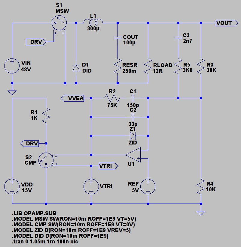
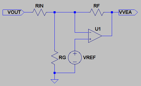
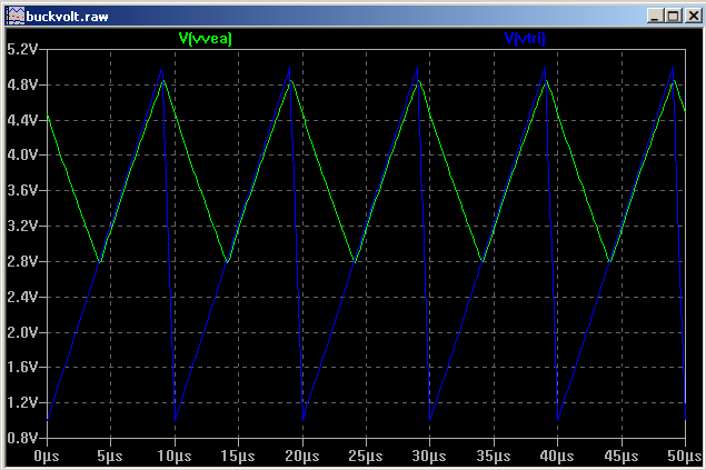
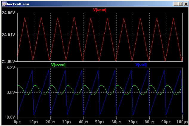
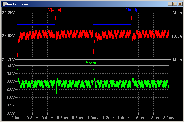
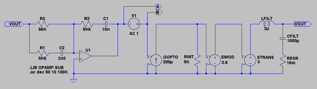
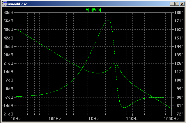
I am using type II amplifier feedback control in my forward converter design, I have been experimenting with output capacitors, increasing ESR of output cap increases crossover freq, reducing gain and phase too. I have been unable to successfully restore improved levels by altering any other values in this loop. Any advice/direction to go, I am new to this but very interested to improve my skills.
 

To improve stability, pls try to reduce crossover freq. It will lead to higher phase margin.
 

I have tried unsuccessfully to do this, with a type II amp in mind I guess I'm looking for a zero/pole adjustment to achieve this while keeping a higher ESR cap on the output.
 

I have tried unsuccessfully to do this, with a type II amp in mind I guess I'm looking for a zero/pole adjustment to achieve this while keeping a higher ESR cap on the output.

What does your overall circuit look like? Specifically are you just using voltage mode control for the output or do you have an internal current mode control loop?
 
I have a current mode control loop. Specifically it's an isolated circuit, to measure stability I injected a signal from output sense(via 10 ohm res) which travels through an RC in parallel, I have a voltage reference with typical type II circuitry across and an opto before signal is fed to PWM. I can post the circuit portion later from the lab. I found that with lower ESR caps as I stated earlier that crossover was acceptable as was phase/gain, however increasing ESR (X2.5 times) results in crossover increase etc. Altering the first RC and and the RCC values across the reference somewhat experimentally does not appear to affect crossover..
 
Can you tell me what sort of isolated converter it is, control IC, switching frequency and input/output voltages plus other information you may feel is relevant.... I suppose I don't need specific values of output capacitors and inductors but it means I might come up with something close to your circuit. Otherwise I can just generalise.

I'd guess you are using a TL341. Give me a bit and then I'll post a more complete answer. 16:00/4.00PM?

Genome

---------- Post added at 14:57 ---------- Previous post was at 14:25 ----------

Oooooooops, just picked up your latest post whilst I was writing this. Since you are using some form of current mode control then you might know about slope compensation.

I'll carry on regardless until you get back to me. The following is based on average current mode control but adapted to work with voltage mode control.

Let's say you are just using voltage mode control on a basic buck circuit. The end result will look something like this,


There are 'fundamental' limits to the amount of bandwidth you can get out of any particular buck configuration. Those limits give you the chance to design the loop in a simple way with some precision and derive from the concept of slope matching..

Consider when your switch is off then the output inductor is being reset through VOUT. Its current ramps down at a rate of LOUT/VOUT. That current ramp is converted to a voltage ramp across the output capacitor ESR and appears as ripple voltage on the output.

If the ESR zero is low enough, and for reasonable switching frequencies and low ESR electrolytic capacitors, or worse, it will be, then when your loop crosses over it is effectively a first order LR circuit on its own and will be so up to the switching frequency. That means, if you did not care about precision you could use a zero order amplifier and things would be stable.


The gain at the switching frequency is limited by the slope matching criterion. If the slope at the output of the error amplifier exceed the associated slope of the PWM triangle ramp voltage then you will get 'subharmonic oscillation'.

In the above circuit my triangle wave swings through 4V in 9uS, switching frequency is 100KHz. This gives me a slope of 440,000 V/s. My 300uH choke is reset through 24V giving 80,000A/s which gets converted to 20,000V/s across the output capacitor ESR of 250mR. That gives me the maximum gain through the error amplifier at the switching frequency as being 440,000/20,000 or 22.

In the above circuit that is ultimately set by R5 and R2. If I set C2 to 1p and run an analysis then I get,


You will see that the slopes are, more or less, matched. If you tried to increase the gain in the error amplifier and the upslope on its output exceeded that on the oscillator ramp then having turned off the switch it would be turned on again, and then off, and then on and.... There would be a blur of switching.

If you had a latching modulator then this would not occur but you would get 'subharmonic oscillation'. At best that would involve unequal pulse by pulse pulse widths. It is this that sets the maximum gain in your error amplifier at the switching frequency and then allows you to move on and determine the rest of the compensation components.

Average current mode control ends up with a result that the loop crossover frequency works out to be Fs/2.pi.D where Fs is the switching frequency and D is the operating duty cycle. Does that apply to this situation?

Let's say your modulator ramp amplitude is Vs. Then as the error amplifier output swings from ramp minimum to ramp maximum the duty cycle goes from 0 to 100% so with a given input voltage, VIN, the modulator gain would be,

Gmod = VIN/Vs

That is applied to your LC output filter but there is the ESR of the capacitor in the circuit as well. Above the CRESR zero frequency your circuit is behaving as an LR voltage divider so,

Sorry Slipped Fingers Not Complete Yet

Gfilt = RESR/(XL + RESR)

Being 'dangerous' I'll simplify that to,

Gfilt = -j.RESR/2.pi.f.L

Then, having waved fingers before, we have to come up with the proper sums for working out the error amplifier gain.

Inductor current slope,

dIL/dT = VOUT/L

ESR voltage slope,

dVESR/dT = RESR.dIL/dT
dVESR/dT = RESR.VOUT/L

Multiplied by the voltage error amplifier gain to get,

dVVea/dT = Gcea.RESR.VOUT/L

Modulator ramp slope,

dVs/dT = Vs.Fs

For slope matching,

dVvea/dT = dVs/dT

So,

Gcea.RESR.VOUT/L = Vs.Fs

Re-arrange to get Gcea as,

Gcea = Vs.Fs.L/RESR.VOUT

Putting them all together to get the Loop Gain,

GL = Gmod.Gfilt.Gcea
GL = VIN/Vs x -j.RESR/2.pi.f.L x Vs.Fs.L/RESR.VOUT

Cancelling things.

GL = -j.VIN.Fs/2.pi.f.VOUT

Then for a buck converter VOUT/VIN is the steady state operating duty cycle D and so,

GL = -j.Fs/2.pi.f.D

Then set GL to 1, throw away the -j, and re-arrange to get the unity gain crossover frequency as,

fco = Fs/2.pi.D

Which is the same result that you get from average current mode control with slope matching but this time it is applied to a voltage loop based on the output capacitor's ESR using the same slope matching criterion.

More in a bit

OK. Having set things up for slope matching then with a DC path around the error amplifier we get no DC precision at the output. At the moment the circuit is 'nominally' first order and stable at crossover. If we want DC precision then we have to break that path, in this case with C1. That will make the circuit second order below the C1/R2 zero frequency which we place at half the 'known' crossover frequency.

Given VIN = 48V and VOUT = 24V then D is 0.5 and with Fs at 100KHz then fco is about 32KHz. That places the zero at 16KHz so, with R2 at 75K, C1 becomes 132pF and I'll use 150pF.... I can see I've made some whoopsies whilst playing so I'll correct the original circuit diagram. Cough.

Then I add C2. Ideally it is just there for 'noise' suppression but otherwise introduces another pole at about twice the previously calculated crossover frequency. In this case I have used 33pF.

Ignoring the other feedback components on the input the loop is second order up to about 16KHz then first order through crossover at 32KHz up to 64KHz where it becomes second order again. Should be stable.

About C3, R5 and R3..

During start up the supply would/might try to run to 100% duty cycle placing an over-voltage the output. Soft start and other mechanisms may prevent this however including this network in the feedback input slows the rise time. C3 will make the loop first order beginning at the C3/R3 pole. Since it is in the input it becomes a loop zero. That gets cancelled at the C3/R5 zero which being in the input is a pole.

I'm sure I have confused myself now. Anyway, with everything now in place..

The start-up is,


This is the input components limiting output rise time.

In regulation,


Slope matching is no longer apparent since C2 is introducing its pole and changing the VEA output waveform.

25%-75% load transient at 1KHz,


Genome.
 
Last edited:
Thank you so much for taking the time to help me, I will have to go over the info a couple of times I'm sure. Much appreciated.
 

I should highlight that the above deals with pure voltage mode control whereas you have an internal current mode control loop as well so it will not necessarily apply, if at all. I started writing it so I thought I'd finish it. Try and post the information about your actual supply and I'll go through that one as well.

Genome
 
If a current mode control supply is having stability issues, then you're probably doing something wrong. In theory, a simply current mode supply can't be unstable with type 2 feedback. And capacitor ESR usually (but not always) has the effect of improving stability, not harming it, because it puts a zero in the transfer function. What is your switching frequency, and what crossover frequency are you aiming for?
 
As it turns out, this particular design IS voltage mode where ESR was increased on output, sorry for the confusion, we have similar issues in a few different designs. This particular one we use National 5025, freq about 220K and cross-over preferably around 15Khz instead of the 22 we're getting with the increased ESR. Input range 18-75, ~3Vo 20A.
 

As it turns out, this particular design IS voltage mode where ESR was increased on output, sorry for the confusion, we have similar issues in a few different designs. This particular one we use National 5025, freq about 220K and cross-over preferably around 15Khz instead of the 22 we're getting with the increased ESR. Input range 18-75, ~3Vo 20A.
Okay, so increasing the capacitor ESR increases crossover frequency, that makes sense. What does it do to your phase margin? Is it actually oscillating, or does its response just become underdamped?

Also, are you measuring response at maximum input voltage? If not, you probably should, since that should yield your worse case stability.
 
Have you considered setting up a linear model of the converter?

In LTSpice,


GOPT is the opto-coupler. Assuming a 1K input resistor and a current transfer ratio of 20% the value becomes 200uA/V. RINT is the internal pull-up resistor of the LM5025. GMOD is the Modulator/Power switch. With 18V in and 50% duty cycle limit with an internal 2.5V clamp its gain becomes 9/2.5 or 3.6. GTRANS is the transformer. 18V in with 6V out for a final 3V gives a gain of 3.

The circuits voltage feed forward will maintain GMOD against variations in input voltage.

Then..... you run an AC analysis and plot V(a)/V(b) which will give you the loop gain of the circuit..


I have been guilty of fiddling with components to get that result but can explain further if you wish. One of the problems will be that you might target a specific crossover frequency but your filter capacitor ESR and opto-coupler will be subject to manufacturing tolerances and time/temperature variations.

Whilst you might hit your required 15KHz crossover frequency in theory in practice that will be subject to variations... That sort of makes my previous 'ideal' analysis almost worthless.

Is the ESR higher because you have been forced to use different devices or is it, in part, and effort to damp the filter resonance? The circuit should be capable of a higher crossover frequency if you wish to be 'dangerous'.

Genome.

we were restricted to certain capacitors, the decision has been made to live with increased cross-over and ripple, it doesn't affect stability. Incidentally I haven't a great deal of simulation experience, however I have downloaded LT Spice, definitely appears more user friendly. Thanks all for your help.
 

Status
Not open for further replies.

Similar threads

Part and Inventory Search

Welcome to EDABoard.com

Sponsor

Back
Top