palmeiras
Full Member level 6
- Joined
- Feb 22, 2010
- Messages
- 375
- Helped
- 61
- Reputation
- 122
- Reaction score
- 50
- Trophy points
- 1,308
- Location
- South America
- Activity points
- 4,199
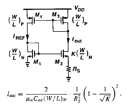
Hello guys,
Please, can someone help me with the following doubts about the traditional PTAT circuit?
(a) How does the positive feedback work in this circuit?
(b) How can I simulate the stability of this circuit using HSPICE?
(c) When the circuit presents a positive feedback, how can I ensure a stable operating point? Sedra Microelectronics book says that making K > 1.0 avoid instability. For me it is not clear. I know that making K higher than 1 we have Iout different than zero, but this does not explain the stability issue.
Thank you very much in advance,
Best regards,