Kit_Leong
Newbie level 2
how to analyze transient response of chopper stabilized bandgap reference circuit?
Hello,
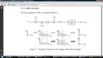
I am currently trying to design a chopper stabilized bandgap reference circuit using tsmc 0.18u technology in mentor graphics.Attached is a journal that shows a full schematic of what I am designing(figure 4) as well as a more basic bandgap without chopper stabilization (figure 3) in which I have already managed to successfully implement figure 3.
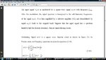
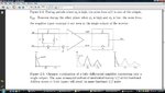
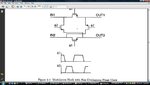
The problem I have now is moving on to figure 4.For the modulator and demodulator,I am using MOSFET's as my switches(as depicted in the Paint screen shot entitled '4 transistors as switches',these transistors will be driven by a square wave pulse alternating between -1 and +1 to perform the modulation and demodulation of the signal and to remove the 1/f noise with the help of a low pass filter)
I tried using NMOS for my switches but it is always in the subthreshold region,even after modifying the width and length ratio.How do I get it into linear or saturation?I tried using PMOS instead of NMOS instead,and I managed to get it to always be in a linear region at the default W/L ratio of 5/2.Does a PMOS function well as switches at linear region?Also,the bulk of a NMOS is usually grounded,while for the PMOS the bulk is connected to a VDD,does that mean I have to connect my bulk to a VDD as well for this 4 PMOS configuration for switching?
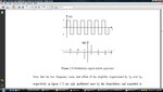
Also I would like to ask what are the expected transient waveform would be like to show that my bandgap is actually chopper stabilized.I have also attached the expected waveforms of chopper stabilized circuits and some explanation on it,but it is in the frequency domain.I would like to know its transient response instead as I do not know how to plot it in the frequency domain,as well as my lecturer has advised me to do it in the transient domain as he also said I can't do it in the frequency domain.I'm not sure why exactly he said I can't do it in the frequency domain,probably due to some limitation in mentor graphics I suppose.But as long as I can prove it is chopper stabilized,I am fine with either transient or frequency domain.Please help.
Thanks.
Hello,
I am currently trying to design a chopper stabilized bandgap reference circuit using tsmc 0.18u technology in mentor graphics.Attached is a journal that shows a full schematic of what I am designing(figure 4) as well as a more basic bandgap without chopper stabilization (figure 3) in which I have already managed to successfully implement figure 3.
The problem I have now is moving on to figure 4.For the modulator and demodulator,I am using MOSFET's as my switches(as depicted in the Paint screen shot entitled '4 transistors as switches',these transistors will be driven by a square wave pulse alternating between -1 and +1 to perform the modulation and demodulation of the signal and to remove the 1/f noise with the help of a low pass filter)
I tried using NMOS for my switches but it is always in the subthreshold region,even after modifying the width and length ratio.How do I get it into linear or saturation?I tried using PMOS instead of NMOS instead,and I managed to get it to always be in a linear region at the default W/L ratio of 5/2.Does a PMOS function well as switches at linear region?Also,the bulk of a NMOS is usually grounded,while for the PMOS the bulk is connected to a VDD,does that mean I have to connect my bulk to a VDD as well for this 4 PMOS configuration for switching?
Also I would like to ask what are the expected transient waveform would be like to show that my bandgap is actually chopper stabilized.I have also attached the expected waveforms of chopper stabilized circuits and some explanation on it,but it is in the frequency domain.I would like to know its transient response instead as I do not know how to plot it in the frequency domain,as well as my lecturer has advised me to do it in the transient domain as he also said I can't do it in the frequency domain.I'm not sure why exactly he said I can't do it in the frequency domain,probably due to some limitation in mentor graphics I suppose.But as long as I can prove it is chopper stabilized,I am fine with either transient or frequency domain.Please help.
Thanks.
Attachments
-
original chopper journal.pdf147.6 KB · Views: 130
-
 chopper frequency domain results.jpg95.2 KB · Views: 158
 -
 chopper frequency domain results explanation 1.jpg118.1 KB · Views: 193
 -
 chopper frequency domain results explanation 2.jpg86.8 KB · Views: 180
 -
 chopper frequency domain results explanation 3.jpg86.2 KB · Views: 186
 -
 modulator,demodulator.jpg127.2 KB · Views: 203
 -
 4 transistor as switches.jpg75.2 KB · Views: 156
")