Continue to Site

Welcome to EDAboard.com

Welcome to our site! EDAboard.com is an international Electronics Discussion Forum focused on EDA software, circuits, schematics, books, theory, papers, asic, pld, 8051, DSP, Network, RF, Analog Design, PCB, Service Manuals... and a whole lot more! To participate you need to register. Registration is free. Click here to register now.

why are both pull-up and pull-down devices are NMOS

Status
Not open for further replies.

euchee

Newbie level 1
Joined
Jan 6, 2008
Messages
1
Helped
0
Reputation
0
Reaction score
0
Trophy points
1,281
Activity points
1,287
Hi, Experts:

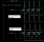
I am looking at one IO buffer design from other Sr person, he used all N devices for both pull up and pull down, please refer to the schematic of attachment.

Everyone says N pull up will reduce swing from VCC to VCC-vth, can anyone explain why he designed this?

Thanks a lot.
 

Attachments

  • clnk_buffer.jpg
    clnk_buffer.jpg
    100.9 KB · Views: 100

NMOS have a much higher conductance per layout area.
Discrete NMOSFETs are much cheaper per Ron*BV than
discrete PMOSFETs, same reason. So you see NMOS-NMOS
totem poles all the time in power switching. These usually
have a bootstrapped gate drive (high side source referred)
which eliminates the VT-drop problem. The problem may be
in your assumptions about gate drive levels, which are not
shown.
 
  • Like
Reactions: euchee

    euchee

    Points: 2
    Helpful Answer Positive Rating
Status
Not open for further replies.

Part and Inventory Search

Welcome to EDABoard.com

Sponsor

Back
Top