doupg
Junior Member level 1
Hi All,
I am using this book: Basic CMOS Cell Design by Etienne Sicard.
I'm trying to simulate everything for better understanding.
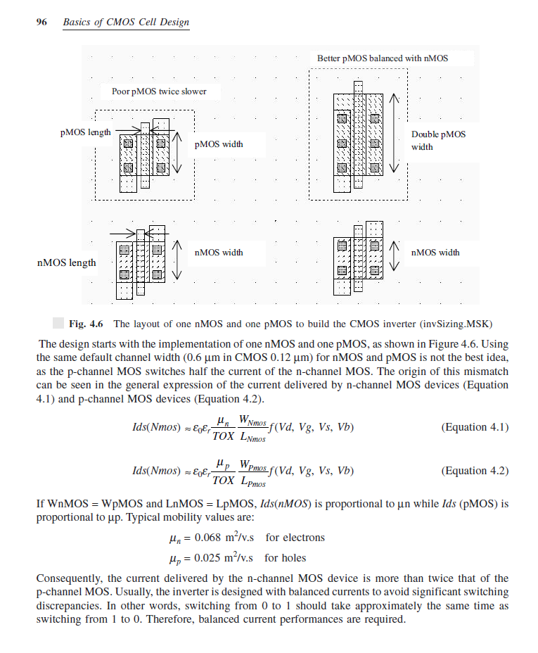
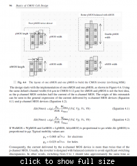
At page 96, Section 4.3 there is an introduction to the "Inverter Layout".
My question is about this:
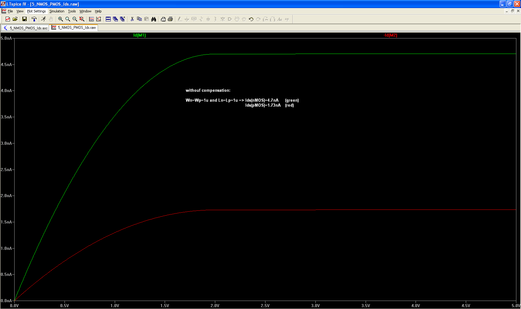
p-channel MOS switches half the current of the n-channel MOS.
I understand the reason:
let's say Width and Large are the same for both nmos and pmos, then we have:
Ids(nmos) is proportional to the mobility of the electrons (Uo=0.068 without units)
Ids(pmos) is proportional to the mobility of the holes (Un=0.025 without units)
which is to say Ids(nmos) is aprox. 2.72 times Ids(pmos).
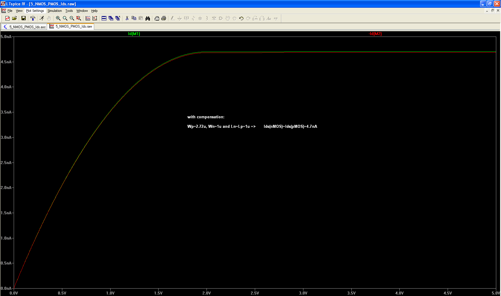
that's the reason why they recommend to use Wpmos=2*Wnmos, to compensate.
Now, I am trying to simulate this to see a difference in the current values (Ion), but that's not the case.
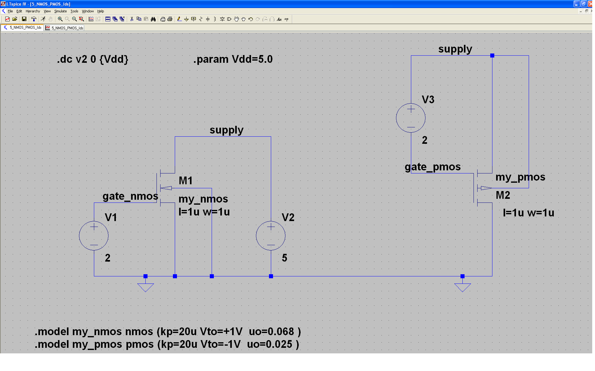
Attached you will find:
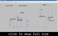
1. spice netlist
2. screenshot of the schematic
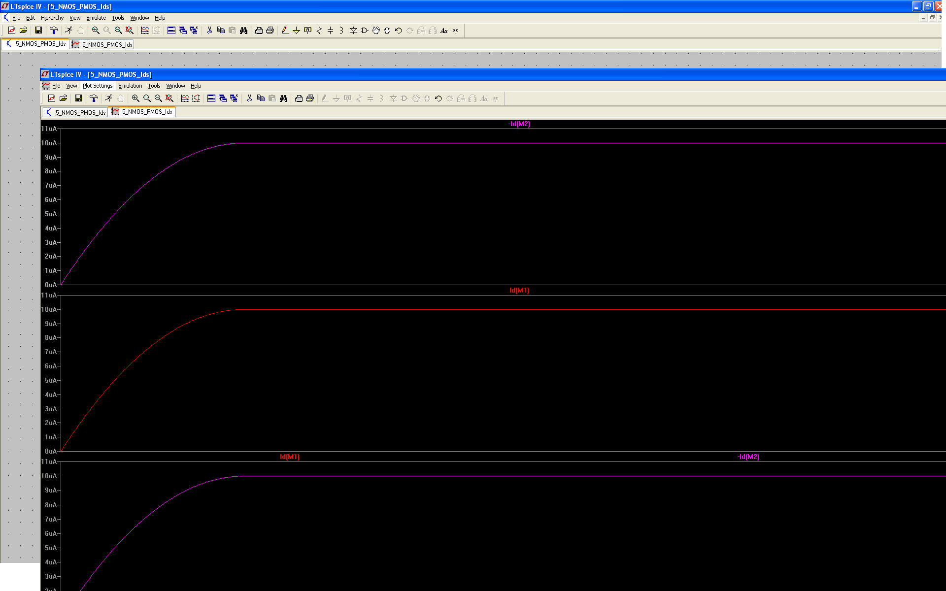
3. screenshot of the simulation results
4. the text that I'm using for study.
So, I was expecting that if Id(M1) (nMOS device)saturates at about 10uA, then Id(M2) (pMOS device) should saturate at about 5uA.
As you can see in my model definition I set the mobility for the pmos and the nmos.
But the results are almost the same.
Thank you for your time and any suggestion.
Best Regards,
here the spice netlist:
V1 gate_nmos 0 2
V2 supply 0 5
M1 supply gate_nmos 0 0 my_nmos l=1u w=1u
V3 supply gate_pmos 2
M2 0 gate_pmos supply supply my_pmos l=1u w=1u
.model NMOS NMOS
.model PMOS PMOS
.lib C:\PROGRA~1\LTC\LTSPIC~1\lib\cmp\standard.mos
.model my_nmos nmos (kp=20u Vto=+1V uo=0.068 )
.model my_pmos pmos (kp=20u Vto=-1V uo=0.025 )
.dc v2 0 {Vdd}
.param Vdd=5.0
.backanno
.end
below the images:
I am using this book: Basic CMOS Cell Design by Etienne Sicard.
I'm trying to simulate everything for better understanding.
At page 96, Section 4.3 there is an introduction to the "Inverter Layout".
My question is about this:
p-channel MOS switches half the current of the n-channel MOS.
I understand the reason:
let's say Width and Large are the same for both nmos and pmos, then we have:
Ids(nmos) is proportional to the mobility of the electrons (Uo=0.068 without units)
Ids(pmos) is proportional to the mobility of the holes (Un=0.025 without units)
which is to say Ids(nmos) is aprox. 2.72 times Ids(pmos).
that's the reason why they recommend to use Wpmos=2*Wnmos, to compensate.
Now, I am trying to simulate this to see a difference in the current values (Ion), but that's not the case.
Attached you will find:
1. spice netlist
2. screenshot of the schematic
3. screenshot of the simulation results
4. the text that I'm using for study.
So, I was expecting that if Id(M1) (nMOS device)saturates at about 10uA, then Id(M2) (pMOS device) should saturate at about 5uA.
As you can see in my model definition I set the mobility for the pmos and the nmos.
But the results are almost the same.
Thank you for your time and any suggestion.
Best Regards,
here the spice netlist:
V1 gate_nmos 0 2
V2 supply 0 5
M1 supply gate_nmos 0 0 my_nmos l=1u w=1u
V3 supply gate_pmos 2
M2 0 gate_pmos supply supply my_pmos l=1u w=1u
.model NMOS NMOS
.model PMOS PMOS
.lib C:\PROGRA~1\LTC\LTSPIC~1\lib\cmp\standard.mos
.model my_nmos nmos (kp=20u Vto=+1V uo=0.068 )
.model my_pmos pmos (kp=20u Vto=-1V uo=0.025 )
.dc v2 0 {Vdd}
.param Vdd=5.0
.backanno
.end
below the images: