Continue to Site

Welcome to EDAboard.com

Welcome to our site! EDAboard.com is an international Electronics Discussion Forum focused on EDA software, circuits, schematics, books, theory, papers, asic, pld, 8051, DSP, Network, RF, Analog Design, PCB, Service Manuals... and a whole lot more! To participate you need to register. Registration is free. Click here to register now.

channel charge injection of Transmission Gate

Status
Not open for further replies.

abcyin

Full Member level 4
Joined
Apr 15, 2005
Messages
236
Helped
12
Reputation
24
Reaction score
3
Trophy points
1,298
Activity points
2,855
Hi, all,

I'd like to reduce the channel charge injection of the transmission gate, I know that this effect could be reduced by selecting the right size of NMOS and PMOS carefully, but this is only for a specific input voltage. When the input voltage changes, the channel charge injection still suffers the output, so could anybody give me some hints on how to further reduce this issue?

thanks in advance.
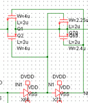
 

I cannot quickly find a reference to it, but you can use dummy transistors to try to cancel it out. In theory I think they should be half the size although due to differences between drawn & effective widths/lengths they values may work out slightly different. See Q69/Q70 in this diagram.

Keith.
 

Attachments

  • Charge injection.gif
    Charge injection.gif
    3.7 KB · Views: 302
You can compensate charge injection -for a given operating
point- by cancellation, but common mode voltage position
becomes common mode charge. So one trick is, try to do your
switching at virtual ground points. Or at low impedance nodes
where charge has somewhere to go. Or make FET gate
overdrive/underdrive fixed values that track the more sensitive
of the two nodes, so that cancellation can be done better
(this can be elaborate and cost power, but it improved one
JFET S/H I worked on, big time for hold pedestal).
 

Another solution is to bootstrap your switch. with TG switch or with NMOS/PMOS channel charge depends on the input voltage. With the bootstrapping you can atleast make the it independent of input voltage and then make it appear as common mode signal to the succeeding stage OTA so that it gets rejected.
 

Status
Not open for further replies.

Part and Inventory Search

Welcome to EDABoard.com

Sponsor

Back
Top