Continue to Site

Welcome to EDAboard.com

Welcome to our site! EDAboard.com is an international Electronics Discussion Forum focused on EDA software, circuits, schematics, books, theory, papers, asic, pld, 8051, DSP, Network, RF, Analog Design, PCB, Service Manuals... and a whole lot more! To participate you need to register. Registration is free. Click here to register now.

FPGA SPI controller no microprocessor

Status
Not open for further replies.

sebas

Junior Member level 2
Joined
Oct 7, 2009
Messages
23
Helped
0
Reputation
0
Reaction score
0
Trophy points
1,281
Activity points
1,468
HI,

I have a design in which I used the FPGA to access an outside the FPGA IC through SPI interface.
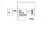
On the FPGA I have a SPI master controller. The SPI controller has the SPI interface signals on one side (that accesses the IC's registers) and a address and data bus (sometimes Wishbone) on the other side. Now I want to put the information read by the SPI controller inside a RAM. The normal approach, for me, would be to use a microprocessor that connects to the SPI controller, on one side, and to the RAM on the other side. The microprocessor would read the SPI controller registers and write them in the RAM. Is there a more simpler approach in which the microprocessor is not needed? Maybe a controller that does the job?

Thanks!
 

Yes, I saw that thread but it doesn't answer my question. I have a SPI Master controller. I want to write the information read from the SPI slave to a BRAM. My question was how do i do that without a microprocessor initiating the transfer.
 

Sorry i'm nor clear to what you need,
i read your post again, you say you have spi controller to your fpga so i guess you can read and write to the slave spi device,
do you mean that you need an internal ram controller that transfers the spi data to the ram, i guess this can be possible using internal signal but you say that the ram is on one side of the fpga and the spi on the other, I'm confused , why can't these two communicate?

Alex
 

Please see attached image. I think you got it right with the ram controller. but how does the ram controller connect to the spi core?
 

Attachments

  • SPI_BRAM.jpg
    SPI_BRAM.jpg
    11.6 KB · Views: 134

Unfortunately i have never used BRAM or know anything about it,
but maybe someone else has an answer now that its clear what you need.

Alex
 

I don't think it's really about the BRAM. It could be an external RAM. My feeling is that I don't understand something simple. Maybe the idea is to design my own core so that it just writes to RAM directly instead of the opencore.org cores where the SPI controller writes the read information in some internal registers that are to be accessed via an address and data bus.
 

I have only used spi with avr controllers but is shouldn't be very difficult.

If fpga is a master and the other device is the slave you have to
enable the slave, send a clk of a low frequency supported by the slave and for each rising or falling edge of the clock (depends on the configuration) you write one bit in the output and you read one bit in the input,
in the end of the byte (depending on the device, some need 2 or 3 bytes) you
deselect the slave (normally pull up the line)

I think you can do it with a state machine,
define a byte to be written and a byte to be read
signal byte_in : std_logic_vector(7 downto 0)
signal byte_out : std_logic_vector(7 downto 0)

then use a process triggered with a clock at the spi frequency and write one bit while you read one bit.

define a miso :in and mosi :eek:ut and also spi_clk :eek:ut and in every clk_spi

byte_in(0) <= miso; (depends if it is MSB or LSB first)
mosi <=byte_out(0);

in the next clock
byte_in(1) <= miso;
mosi <=byte_out(1);

until you send/get the byte, then write this byte to the ram

Alex

---------- Post added at 16:25 ---------- Previous post was at 16:18 ----------

Also look at this **broken link removed**

Alex
 
  • Like
Reactions: sebas

    sebas

    Points: 2
    Helpful Answer Positive Rating
BRAM is just standard Xilinx Block RAM. Look at the the Xilinx datasheet for BRAM to get an idea of the timing diagrams for reading and writing. Then write an RTL module that takes the serial SPI data and then writes it to the BRAM as parallel data.
 
  • Like
Reactions: sebas

    sebas

    Points: 2
    Helpful Answer Positive Rating
Status
Not open for further replies.

Similar threads

Part and Inventory Search

Welcome to EDABoard.com

Sponsor

Back
Top