Continue to Site

Welcome to EDAboard.com

Welcome to our site! EDAboard.com is an international Electronics Discussion Forum focused on EDA software, circuits, schematics, books, theory, papers, asic, pld, 8051, DSP, Network, RF, Analog Design, PCB, Service Manuals... and a whole lot more! To participate you need to register. Registration is free. Click here to register now.

555 based pwm train controller

Status
Not open for further replies.

mvagusta

Junior Member level 2
Joined
Jan 17, 2008
Messages
21
Helped
1
Reputation
2
Reaction score
1
Trophy points
1,283
Activity points
1,470
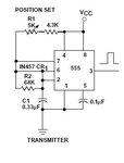
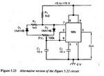
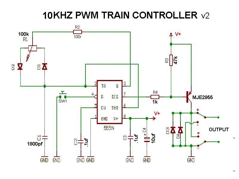
Hi everyone, I'm looking at making a model train controller based off this circuit:

**broken link removed**

I'm thinking that by changing C1 to 1800pf/1.8nf, the PWM frequency should be up around 10khz? These little trains run really smoothly with PWM up this high.

circuit.gif


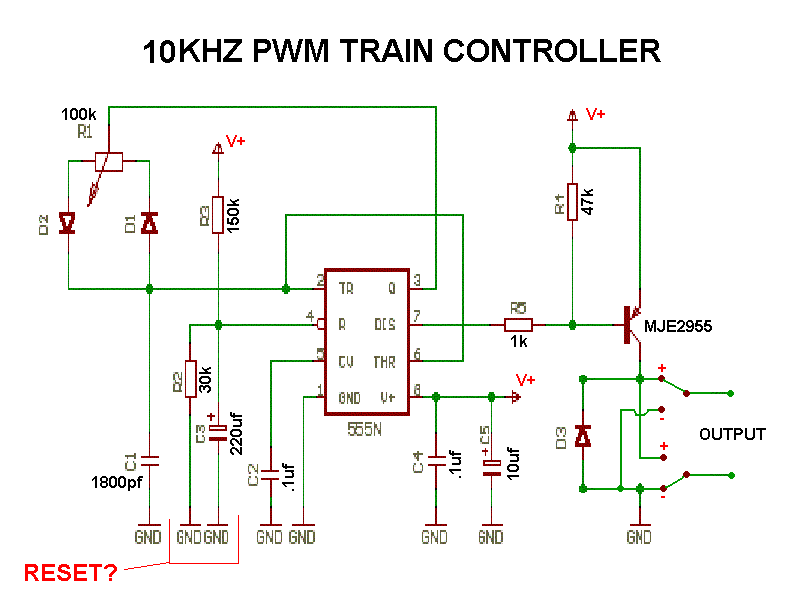
The kickstart has a reset time of ~2 seconds, but I think I can get that down to just under 1 second by changing C3 from 220uf to a 100uf instead?

The other thing is, how do I engage the kickstart??? Is it by connecting both R2 and C3 to ground?

I've also added a DPDT reversing switch for the output, and a MJE2955 transistor instead, since it's nearly as cheap as the original BD140 and has a 10A rating, so it will handle the trains easily.

I'm also thinking to add another diode in parrallel with the output diode, for redundant protection against back emf from the model train engines. Good idea?

I think I should also add an inductor to the output, after the reversing switch, something a little beefy with ~1mm thick wire and ~.5 ohm resistance, for some short circuit protection.
 

Hi
I am not sure if you really need the R2 resistor(30K). This is because the reset pin is generally high, its only when one has to reset the IC one makes it low. With the R2 and R3 potential dividing network the voltage at pin 4 shall be about 0.1666 Vcc which will keep 555 in reset state. In case you need to give an initial delay remove R2 (which I suppose is a bleeding resistor) or swap R3 and R2 if you really need a bleeding resistor.

Also I think the circuit is flawed or its a very strange way of using NE555, as the functionality of pin 3 and pin 7 of the ic are interchanged. Pin 3 is the output and the PWM should be visible on this pin and pin7 is the discharge pin.

Lastly the the potential divider R1 should be some way connected to VCC.

I have attached the general configration in which NE555 is used as a PWM generator. For more info check the data sheet of the IC.

Asimov
 

Attachments

  • pwm-motor.JPG
    pwm-motor.JPG
    10.8 KB · Views: 214
Last edited:
Also I think the circuit is flawed or its a very strange way of using NE555, as the functionality of pin 3 and pin 7 of the ic are interchanged. Pin 3 is the output and the PWM should be visible on this pin and pin7 is the discharge pin...Asimov
Previously before seeing the below mentioned website, i too thought it should be a design error. But it is possible to use the 7th pin of 555 as an output, and "easterngeek" as done it and prooved it on youtube video. I was about to give the circuit a try but expect some experienced friend to guide me about how it works and whatz the principle behind it.
**broken link removed**
https://www.youtube.com/watch?v=MWs30OfWSts
 
I have attached the general configration in which NE555 is used as a PWM generator.
However, the below published circuit is much better in controlling the duty cycle. So it wouldn't be a good idea to use your circuit instead.

The other point ist, that "output" and "discharge" pin are obviously carrying the same signal, in so far they are exchangeable. There are actually many ways to achieve a similar functionality. As long as a particular circuit isn't violating the maximum ratings of a device or not working reliably for some reason, you shouldn't tell it's flawed. At least not, before completely understanding it's operation.
 
Hi,
Well I gave it another thought, yes it is possible to use the discharge pin as out put Pin because discharge pin is actually the collector pin of a transistor with the emitter gounded and the base connected to the RS flipflop but when using pin 7 as output there is a serious limitation, the limitation is that when using pin 7 as output you can only sink current(that too a limited amount so as not to burn the discharge transistor) where as when one uses the pin 3 as output one can source and sink current upto 200mA .

Ahh, one good thing to point out about this circuit is that it should be able to generate perfectly symmetric square wave(having equaly high and low period) where as in usual configration no matter what you do you can never reach the 50% duty cycle. But here comes a word of caution , I think there should be a safety resistor between the wiper of the potentiometer and the pin 3 . This is because pin 3 will be swinging between +vcc and gnd and in case the potentio meter is at it extremes end this will be a situation where the capacitor charging or discharging loop will have a very low resistance path. This is not a very good situation from design perspective(I may call it flawed in this respective).

Definately the other issues pointed out remain as they are(or I will have to think deeper about them as well). The reset pin being pulled close to ground level.


I am attaching a more precise version of the circuit , this is from a book Timer Generator Circuits by R.M Marston.
Asimov
 

Attachments

  • PWM1.jpg
    PWM1.jpg
    58.9 KB · Views: 290
Last edited:
Thanks for all the help guys :-D

Here's the link to the original of this circuit: **broken link removed**

Am I correct that by changing C1 from .1uf to 1800pf/1.8nf, the PWM frequency would change from ~200hz to approximately 10khz? These little trains run really smoothly with PWM up this high.

I'm thinking that I can remove R2, R3, and C3, and just have a momentary switch to connect pin 4 to ground?
And just to confirm, whenever pin 4 is connected to ground, a continous/100% duty cycle 12v dc would be delivered to the output?

It's ok if the circuit can only generate up to 50% duty cycle via the variable resistor. It's much more important that it's able to go all the way down to 0% duty cycle, so we can smoothly controll the train at low speed, and bring the train to a stop.

A safety resistor sounds good asimov, how big should it be?

edit: I just saw that circuit you posted asimov, what duty cycle range can that one produce?
 

I think there should be a safety resistor between the wiper of the potentiometer and the pin 3
I also tend to place current limiting means in similar situations. But as you already found out, the discharge open collector has basically the same output characteristic as the output pin, and it's commonly connected to larger timing capacitors, apparently without a need for current limiting, see the datasheet's application circuits for reference. I didn't yet hear of failing LM555 standard circuits. But for a well founded design, we should have SOA characteristics of the output transistors, that aren't given.
 
I threw in a 100 ohm resistor from the wiper to pin 3, and just used a momentary switch from pin 4 to ground to trigger reset/full power output. How's it look now?

PWMv2.gif


Could someone also please tell me if the PWM frequency of this circuit would be ~10khz?

I dunno what SOA characteristics are, but I'm planning on using the relatively beefy MJE2955 to drive my boy's little N scale train, that uses from 300ma up to 500ma under load.
 
The PWM frequency will be about 1/(0.69*100k*1.8 nF) = 8 kHz. The SOA (safe-operating area) comment was related to the LM555 transistors and the safety resistor problem. SOA can be also a topic for your power switch, but I guess it's O.K.

I dodn't understand the purpose of the reset push-button. Without a delay capacitor, the reset is effectively useless in this application. And I won't leave the reset input floating, if not tied to VCC, place a pull-up resistor.

As an additional point, the MJE2955 will be switched-off very slowly by the 47k resistor and generate more losses than necessary. And the base current set by 1k resistor isn't sufficient to drive a load higher than a few 100 mA at guaranteed MJE2955 current gain.
 
Last edited:
Hi

I completely agree with FvM. The frequency will be about 8KHz and the floating reset pin(better pull it up with a 4.7K Resistor). Also preferably change R2 to 1K rather than 100 Ohms.


Asimov
 
Thanks heaps for all the help guys.
 

Status
Not open for further replies.

Similar threads

Part and Inventory Search

Welcome to EDABoard.com

Sponsor

Back
Top