Continue to Site

Welcome to EDAboard.com

Welcome to our site! EDAboard.com is an international Electronics Discussion Forum focused on EDA software, circuits, schematics, books, theory, papers, asic, pld, 8051, DSP, Network, RF, Analog Design, PCB, Service Manuals... and a whole lot more! To participate you need to register. Registration is free. Click here to register now.

High Side Driving Trouble

Status
Not open for further replies.

khansaab21

Advanced Member level 4
Joined
Apr 12, 2008
Messages
108
Helped
4
Reputation
8
Reaction score
2
Trophy points
1,298
Activity points
2,214
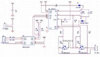
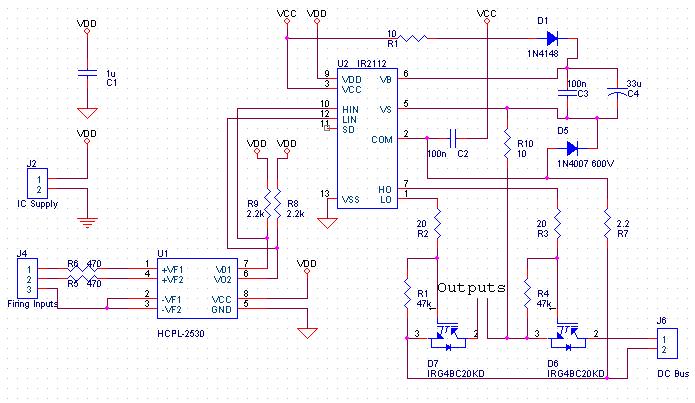
Hello guys, following is my circuit representing a single phase of a three phase inverter for driving a three phase AC induction motor.


The isolators are reproducing the PWM inputs nice and smooth. Low side is running good. Low side is driving the load as intended. (I have tested it using DC motor as a load connected between collector of low IGBT and Vcc and the speed was varying proportional to PWM).

The problem relies with the high side. It is not driving the load AT ALL. Following are some of the facts that I can observe in the circuit. High side supply is 15V and low side is 12V. The input is PWM at 20kHz. The output is between emitter of high side IGBT and ground.

1. VB pin doesnt go beyond 12V.
2. HO pin carries 10V, at no load condition.
3. HO pin drops to 0.8 V as soon as load gets connected.

Is there a problem in the circuit or I am missing something??
 

D1 must be a fast, high voltage diode with a rating according to the bus voltage. In the schematic, the connection between D7 C and D6 E is missing.
 

D1 is fast enough with reverse recovery time of around 4 ns. And at the moment I am driving the high side and low side IGBT's in independent mode. And as mentioned, low side is working but high side is not. I have even tried the way you have said but still no change in the results.

I need to get this part of project completed as the dead line is coming nearer day by day.
 

At the moment, I am only using 12 V and 15 V, (and 24 V in my university lab) for testing purposes. So, it really should not be a problem for now. But the point is, if the VB pin is not going above 15V, then how is it going to fire the IGBT on?? So far I havent found any relevant answers on the internet about the sources and causes of this sort of problem.

By the way, I didnt know that 1N4148 is only good up to 100V. This point is gonna help me when I finally connect the AC motor. BUT, thats only gonna happen when I get through this problem.

---------- Post added at 20:41 ---------- Previous post was at 20:14 ----------

Could you please tell me a way to verify, that either this circuit even performing boot strapping or not??
 

Operating the circuit at a low bus voltage makes safe desktop much easier, of course.

Generally, the bootstrap circuit can work at any bus voltage (including zero) as long as the VCC supply is sufficient (e.g. 12 V) and the duty cycle is somewhat below 100%, in other words, the on-time of the low side switch is sufficient to charge C3/C4. By adding R1 and R10 to your circuit, the allowed maximum duty cycle is reduced, because it takes more time to charge C3/C4. Monitoring the voltage between VB and VS (differential measurement required) is the basic point for checking the bootstrap operation. If it drops below the low voltage detector threshold, the circuit operation will fail.

In your schematic, no VCC supply source is shown.
 

The schematic shows an open jumper to the DC bus. Is
that taken care of?
 

As a matter of fact, the system has started responding now in both high and low side configurations. And this all started happening as soon as I changed the gate driver IC. So I guess, that particular piece of IC was problematic OR I had damaged it by performing extensive testing in order to make the system work.

---------- Post added at 20:07 ---------- Previous post was at 20:03 ----------

Also, as told by FvM and dick_freebird, boot strapping isnt going to happen if the connection between D7 C and D6 E is missing. But, I had an impression by reading the data sheet that both high side and low side outputs can be managed independently. Hence for testing purposes I didnt make that connection.
 

probably was the heat of the solder gun if you did this by hand.
- i would change R1 and R4 to 5K. just helps turn off faster when you suddenly lose control voltage.
- C4 should be film type cap, definitely not electrolytic. you need a cap that can discharge fast, charge fast, and have little internal impedance.
- J4, looks like you intended to supply the driver chip, but the ground is different. could be a type-O?
- put a 0.1u in parallel with C1, the dV/dT of your switch will create high frequency (>1MHz) noise.
- this is just my habbit.. but i would put another gate resistor of same value in parallel with R2 (& R3) . then also add a D4148 with cathod pointing towards driver chip. this give you the opportunity to tune the turn ON/OFF separately from each other.
- R2 and R3 should be placed as close to the mosfet as possible, with the drive chip and big cap also close by. minimize the loop distance. those resistors R2, R3 are usually hard to cool.. they get hot and they are not on a heatsink (too much parasitic capacitance to ground, so not connected to a cold plate). therefore, they should be way over designed.. i.e. if you calculate 1W resistor.. put a 5W. ..

Mr.Cool
 
Last edited:
- I havent soldered the circuit yet, so that fault wasnt due to soldering. I was just testing on bread board. Maybe I shorted out some pin during making connections and that hurted the chip

- The 100n capacitor is 'myler film' type while 33u is electrolytic. And this combination was working well. I have even tried the 100n ceramic type capacitor. But all of this was on 15V floating supply (and 12V DC motor for testing purposes). The target motor is 230Vac induction motor. I hope this wont be a problem with induction motor too.

A question arises from this point, that what should be the voltage rating of C3 and C4. I am using 15V supply for low side while the high side floating supply would be (ultimately) 315V DC. So, either 25V rated C3 and C4 are good enough or the rating should be > 315V ??
 

what should be the voltage rating of C3 and C4
It's charged to 15 - 0.7 V (VCC - one diode drop) at maximum. The same voltage level appears as the highside IGBT Vgs, it definitely won't like more than 20V.
 
Status
Not open for further replies.

Part and Inventory Search

Welcome to EDABoard.com

Sponsor

Back
Top