Continue to Site

Welcome to EDAboard.com

Welcome to our site! EDAboard.com is an international Electronics Discussion Forum focused on EDA software, circuits, schematics, books, theory, papers, asic, pld, 8051, DSP, Network, RF, Analog Design, PCB, Service Manuals... and a whole lot more! To participate you need to register. Registration is free. Click here to register now.

non-overlapping clock generator

Status
Not open for further replies.

allennlowaton

Full Member level 5
Joined
Oct 5, 2009
Messages
247
Helped
3
Reputation
6
Reaction score
3
Trophy points
1,298
Location
Taiwan
Activity points
3,062
Good day EDA fellows...

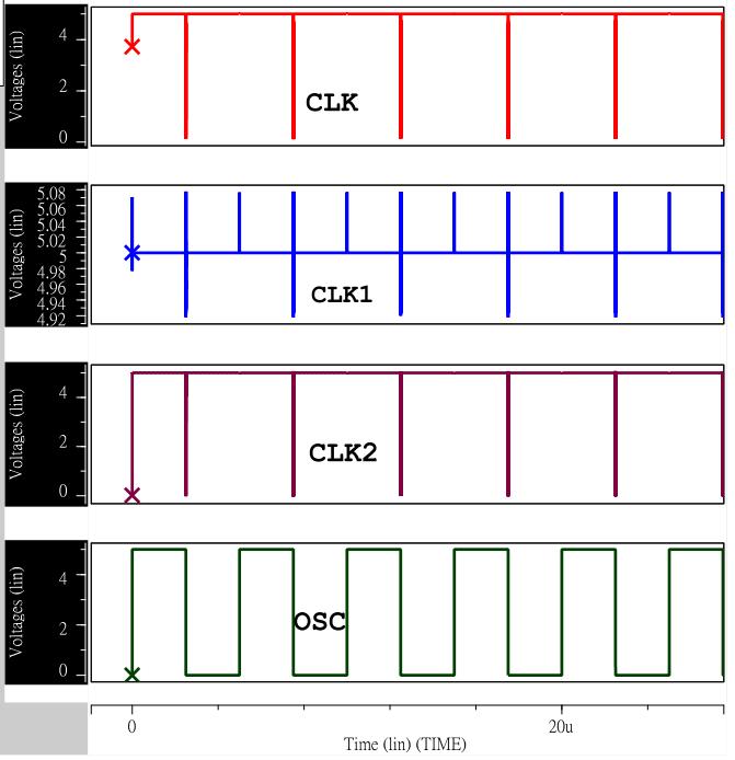
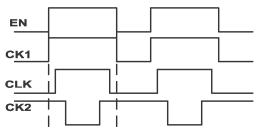
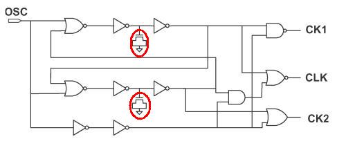
I'm having this 3 output non-overlapping clock generator circuit.
I'm having concern regarding those 2 MOS (drain and source connected). What's their purpose?

Thank you very much for spending time on this thread.

23_1285847056.jpg
 

The transistor are apparently used as capacitors to create an artificial logic gate delay. Obviously, the clock generator operation depends on logic delays, so without knowing all technology parameters and transistor l and w, you can't predict it's output signals.
 
thanks FvM..I had a simulation on this architecture using the minimum sizes but the output is like this...


The result is so weird.
Please give me a starting point to debug this problem.
 

Are you sure you are simulating the right thing? It looks like the OSC input is an enable signal. When OSC=0 then the NOR gates on the left work as inverters. Hence you have a six-inverter ring-oscillator where you take outputs from the 3rd and the 6th inverter. The gates on the right then enable or disable, and fix the phase relation of the output signals (i.e. CK2 goes high (and not low) a bit later than CK1 goes high).
 
@kgl_13gr: I used a pulse input for the OSC. I expect the output should be like the one below.
I also got confused what to use for that MOS that acts as capacitor. What should be its size?

75_1285940276.jpg
 

why concern?!
you can omit these transistors (which has been used as capacitor to cause a more non-overlapping delay.) this regards to your desired specifications of output signals as NOL clocks.
 
Status
Not open for further replies.

Similar threads

Part and Inventory Search

Welcome to EDABoard.com

Sponsor

Back
Top