Continue to Site

Welcome to EDAboard.com

Welcome to our site! EDAboard.com is an international Electronics Discussion Forum focused on EDA software, circuits, schematics, books, theory, papers, asic, pld, 8051, DSP, Network, RF, Analog Design, PCB, Service Manuals... and a whole lot more! To participate you need to register. Registration is free. Click here to register now.

switched-capacitor circuit need your help

Status
Not open for further replies.

lhlbluesky

Banned
Joined
Mar 30, 2007
Messages
558
Helped
5
Reputation
10
Reaction score
5
Trophy points
1,298
Location
china
Activity points
0
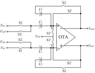
i have designed a sc circuit, as the figure shows, Cs=Cf, Vout=Vout+ - Vout- = (Vin+ - Vin-) - (Vref+ - Vref-), Vin = Vin+ - Vin- = (0V~2V), Vref = Vref+ - Vref- = 1V, Vout = Vout+ - Vout- = (-1V~+1V), my question is, when the output is small (150mV or small), the settling accuracy decreases a lot, for example: when (Vin+ - Vin-) - (Vref+ - Vref-) = 1.2V, the settling accuracy is 14bit (Vout = 1.19994V), but when (Vin+ - Vin-) - (Vref+ - Vref-) = 100mV, Vout = 99.85mV (9 bit accuracy), when (Vin+ - Vin-) - (Vref+ - Vref-) is even smaller, the settling accuracy is 8bit or less, why? what is the possible reason?

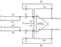
Cs=1.3pF, opamp is two stage (fold cascode + common source) with cascode compensation.

please help me, thanks all.


can anyone help me, or give me some suggestions?
 

Without seeing your OTA design, my guess would be that it`s a bias issue.
Check that all your transistors are in saturation for the problematic input voltage.
If that doesn`t help you find the issue,
maybe you can post your schematic and I can try to find the problem.
Hope this helps.
 

I assume you use non-overlapping clocks to minimize input dependent charge injection?
 

Status
Not open for further replies.

Similar threads

Part and Inventory Search

Welcome to EDABoard.com

Sponsor

Back
Top