Continue to Site

Welcome to EDAboard.com

Welcome to our site! EDAboard.com is an international Electronics Discussion Forum focused on EDA software, circuits, schematics, books, theory, papers, asic, pld, 8051, DSP, Network, RF, Analog Design, PCB, Service Manuals... and a whole lot more! To participate you need to register. Registration is free. Click here to register now.

How to use Xilinx ISI Software

Status
Not open for further replies.

moonnightingale

Full Member level 6
Joined
Sep 17, 2009
Messages
362
Helped
5
Reputation
10
Reaction score
5
Trophy points
1,298
Activity points
3,832
I am having this simple code

module andgate (a, b, y);
input a, b;
output y;
assign y = a & b;
endmodule

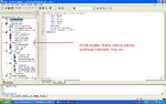
I want to run this code in Xilinx ISI Software
Can somebody tell me basic steps to run a program in it.
kindly give me all details as i am stuck. its tutorial is also not helpful
i know Verilog but i dont know how to use this software
 

You may refer this quick start tutorials from xilinx
 

Attachments

  • qst_2.pdf
    569.5 KB · Views: 113

just start a new project. select verilog as the language.then keep on clicking next until u get the window. then select new source and select verilog module
.enter inputs and outputs in the tab.then type the code .and do behavioural simulation first . then synthesis
 

Attachments

  • xilinx syn.JPG
    xilinx syn.JPG
    125.7 KB · Views: 129
  • xilinx verilog.JPG
    xilinx verilog.JPG
    120.7 KB · Views: 138
just start a new project. select verilog as the language.then keep on clicking next until u get the window. then select new source and select verilog module
.enter inputs and outputs in the tab.then type the code .and do behavioural simulation first . then synthesis

Thanks a lot. It worked. I am highly grateful to you. I did FPGA Course 4 years back but remained out of touch.
At present i am following book of J Bhasker Verilog HDL Synthesis. but this book does not explain software
Can you send me some site where Xilinx ISE 6 is explained or can u throw some light on left side panel
 

Attachments

  • panel.JPG
    panel.JPG
    150.4 KB · Views: 135

well i dont know too much . i will say what i know .Synthesis is transforming the code into hardware or more aptly fitting code into hardware.
the synthesis report is a collection of reports on timing , area , how many LUT's are used power etc...
If u look up the RTL schematic of the module it will show the block diagram of the module with input and output.U can double click on it until u get to basic gates. kind of interesting to see synthesized diagrams for all of our designs.
the next part is translate and mapping the design.i,e it translates the synthesized design and maps it into corresponding FPGA that u chose at first.the design is mapped to the LUT's of the FPGA.you must assign package pins by seeing the data sheet of your FPGA to the module 's I/O

Hope that helps
 

Status
Not open for further replies.

Part and Inventory Search

Welcome to EDABoard.com

Sponsor

Back
Top