Continue to Site

Welcome to EDAboard.com

Welcome to our site! EDAboard.com is an international Electronics Discussion Forum focused on EDA software, circuits, schematics, books, theory, papers, asic, pld, 8051, DSP, Network, RF, Analog Design, PCB, Service Manuals... and a whole lot more! To participate you need to register. Registration is free. Click here to register now.

Operation of a transistor....

Status
Not open for further replies.

Urmi

Junior Member level 2
Joined
Jun 4, 2010
Messages
22
Helped
0
Reputation
0
Reaction score
0
Trophy points
1,281
Location
India.
Activity points
1,476
Please, please ,please answer...
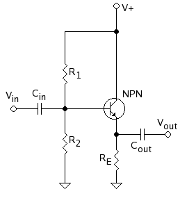
1.Why do we compare Beta and alpha values for CE configurtion?Only alpha matters in this config,doesn't it.but then why do we find the realation betwen alpha and beta?

2.does the value of beta vary with the input voltage? Why?

3.The output resistance in CE and CC are both defined as (Vbe/Ib),but in CE,it has a low value (around 750 ohm)and in CC it has very high values (750 kilo ohm) Why?

(CC,CE,CB are Common collector,common emitter and Common base respectively).

4.The quiescent point is the intersection point of the load line and the output characteristic curves...but there are different curves of Vce vs Ic representing the different values corresponding to different Ib....then which intersection point do we mean while representing the Q point?


(please try to be a little descriptive).
 

AD1 No, in CE only Beta matters.
AD2 Becaues Ic change with input signal.
And changes in Ic change beta.
AD3
(Vbe/Ib) is a input impedance not output.
And CC has a larger Rin becaues Re resistor in emitter.
And for CC Rin is equal Vin/Iin
Simply Ib in CC amplifier is dependent on Ie and Ie depend on Re.
So
Vin = Vbe + Ie*Re = Vbe + Ib*(β+1)*Re
so for DC
Rin = (β+1)*Re
AD4
**broken link removed**
 

jony130 said:
AD1 No, in CE only Beta matters.

Oh...sorry,silly mistake...but then my question is why we derive a relation between beta and alpha,since each of them is important for a different configuration and not simultaneously in any of the configurations.

jony130 said:
AD3
(Vbe/Ib) is a input impedance not output.
And CC has a larger Rin becaues Re resistor in emitter.And for CC Rin is equal Vin/Iin

I didn't understand the bolded part.

Thanks for the reply....please clear my doubts before I end the topic.
 

2.does the value of beta vary with the input voltage? Why?

Urmi, in amplifier circuits it is absolutely necessary to discriminate between dc voltages (for determination of bias resp. operating points) and signal voltages which normally are sinusoidal. Therefore: What do you mean with "input voltage"?
Signal voltages do not (must not!) influence the operating point. Dc bias voltage is used to determine this point since the operating point depends on the selected base resp. collector current (controlled by Vbe).

4.The quiescent point is the intersection point of the load line and the output characteristic curves...but there are different curves of Vce vs Ic representing the different values corresponding to different Ib....then which intersection point do we mean while representing the Q point?

You have the choice! That is the first decision to be made before designing an amplifier. You can choose an operating point (why do you call it Q point?) with higher or lower collector currents by selecting one appropriate Ib curve.
Higher currents give more gain - however the input resistance and the dynamic range is lower/samller. That's a classical compromize to find.
___________
Hope, this clarifies something.

Added after 5 minutes:

jony130 said:
....................................
And for CC Rin is equal Vin/Iin
..................
so for DC
Rin = (β+1)*Re

Hi Joni, please don't mix dc and ac values. This doesn't help at all.
(see my reply to urmi).
 

    Urmi

    Points: 2
    Helpful Answer Positive Rating
answer1
since emitter current is the largest current. alpha=Ie/Ic. it gives the proportion of output current to the input current.
answer2
beta=Ic/Ib so as input changes bet also changes. beta is also effected by temperature
answer4
we have a single Ib curve for single input. so only single Q point. different Ib curves shows the differnt Q point at differnt Ib values.

Ib=base current, Ic=collector current, Ie=emitter current
 

Recommendation to urmi: Forget the above reply. Meanwhile, you know better.
 

Urmi said:
but then my question is why we derive a relation between beta and alpha,since each of them is important for a different configuration and not simultaneously in any of the configurations.
Maybe because we don't get alpha in datasheet.
Only β (Hfe) is specified in the datasheet.
And in reality we don't need alpha for design purpose.
And you can forget what alpha really is.

Urmi said:
jony130 said:
AD3
(Vbe/Ib) is a input impedance not output.
And CC has a larger Rin becaues Re resistor in emitter.And for CC Rin is equal Vin/Iin

I didn't understand the bolded part.
In CC amplifier
Common_collector.png

the emitter of a BJT is connect to the ground by Re resistor.
So input impedance of a CC amplifier is a sum of a input impedance of a BJT without Re resistor (this is the input impedance of a CE amplifier) plus resistance of Re resistor seen by base of CC amlifier.
Rin = Hie + (β+1)*Re
Hie - input impedance of a CE amplifier Hie = β*(26mV/Ic)
 

Its easy to see in this manner:
Vin must be higher than the voltage across Re for current to flow into the base of the transistor.

If we assume the input impedance is (incorrectly) RE, then we would have a large current into the NPN's base.

This would cause a MUCH larger current to flow from collector to emitter. This would cause a higher voltage across RE.

In that case, less current would flow from Vin to RE.

Thus, a change in vin results in a change in I_RE, but such a change requires a much smaller change in the current into the base. This makes the input resistance much higher than just RE.
 

May I add another simple explanation/verification of this effect?
The B-E junction and the resistor seem to be connected in series - however they are not! The reason is: The current through both parts is not the same.
 

Hi everyone! Sorry for not responding back to your posts...I've been having exams
and my Electronics exam got over only today.

LvW said:
Urmi, in amplifier circuits it is absolutely necessary to discriminate between dc voltages ....
Signal voltages do not (must not!) influence the operating point.

Well you see, I was just referring to the plot of Ic vs Vce like we find in typical output characteristics.....in one of the problem sums in my book,they use the term
(beta max)..but I thought that beta was supposed to be constant...no question of beta max or min.

About the Q-point--your post really helped....so now I understand that Q-point is determined as per our requirements,and it is the intersection point of the load line with the output characteristic curve for the selected value of Ib that we want to work with...the intersection point means that we can tell the current and voltage accross the load resistor aswell as the collector all at once.

Added after 10 minutes:

jony130 said:
Maybe because we don't get alpha in datasheet.
Only β (Hfe) is specified in the datasheet.
And in reality we don't need alpha for design purpose.
And you can forget what alpha really is.

Hmm...so if we forget what alpha really is,we could treat the relation between alpha and beta just as a mathematical one,and since we don't get readily specified values of alpha(as you said),we could use it just to find alpha whenever we needed.
jony130 said:
In CC amplifier
Common_collector.png

the emitter of a BJT is connect to the ground by Re resistor.
.....

Okay...I think I'll take a while to figure this out...

Added after 17 minutes:

Hmm...on second thoughts...from our discussion on load lines and Q-points....it suddenly comes to my mind that we have just one straight line plot for a load line,whereas we have multiple curves on the transistor characterisitics...it is said that the load line exhibits all the possible combinations of Ic and Vce...but even along one output characteristic curve (for a particular Ib value),we have lots of different values of Ic and Vce...how can the load line contain all that stuff in just one straight line?

Besides,as I explained in my post,at the Q-point describes the situation for the selected value of Ib and the Ic and Vce values at that point....but Ic-Vce could have lots of different values for a particular Ib value.
 

Hi URMI,

let me start with two simple examples:

1) Two resistors in series: Easy to calculate, no graphic representation necessary, because you know the rules (Ohm's law).
2.) Resistor and diode in series: If you dont want (or cannot) to express the U-I characteristics of the diode as a formula, you must do a graphic solution because of the non-linear diode transfer characteristic. At the same time Ohms law has to be fulfilled by the resistor. That leads to two plots (diode nonlinear, resistor linear) in only one cartesian system (after choice of a supply voltage). The crossing of both curves gives the only possible operating point.
3) Same situation for resistor and C-E path of a transistor in series. However, one difference: You have not only one non-linear characteristic but a variety due to the third controlling node (base). Now, the situation is as follows:
The resistor must (it has no choice) fulfill Ohms law and the transistor must behave according to its non-linear characteristic. Now, you plot - after having fixed the supply voltage and the resistor value - both characteristics in ONE diagram.
The only possible point (operating point) which fulfills both laws is the crossing point.
That's the secret of the load line in the transistor output diagram.
 

Thanks,LvW....
that means that when we have a transistor in series with a resistor,each obeys it's characteristic behaviour...irrespective of each other,(as long as kirchoff's laws along the series connection are obeyed)..at the operating point,they have the same voltage and current accross them...this is taken as a reference(operating point) due to convenience??
 

[quote="Urmi"
....................
..at the operating point,they have the same voltage and current accross them...this is taken as a reference(operating point) due to convenience??[/quote]

The same current - yes. But the sum of both voltages (across CE and across Re) is identical to the supply voltage - however, both are allowed to be equal.
 

    Urmi

    Points: 2
    Helpful Answer Positive Rating
Yes,I guess the voltage accross the resistor and that accross the transistor always have to add up to the applied voltage(kirchoff's law)....but since the operating point is the intersection point of the curves,the value of voltage has to be the same for both.
 

Urmi said:
Yes,I guess the voltage accross the resistor and that accross the transistor always have to add up to the applied voltage(kirchoff's law)....but since the operating point is the intersection point of the curves,the value of voltage has to be the same for both.

No, URMI, that`s not correct.
While mentioning that both characteristics (Ohm for the resistor and the nonlinear curves for the BJT) are to be drawn in one common graph means that the voltage across the resistor has to be expressed by the Vce (i.e. Vres=Vsupply-Vce).
Otherwise, you cannot plot them in one single cartesian system. And that't the only way to find a crossing beween both curves. And therefore, both voltages are NOT necessarily identical. Try it by yourself.
 

Okay,LvW,I understand why the potential accross the resistor and the transistor are not the same......but then what is so special about the 'intersection' of the two curves that we have to choose the operating point there,only?
 

I repeat one sentence from my reply August 17th:

The only possible point (operating point) which fulfills both laws is the crossing point.

OK?
 

Sorry for being so confused over this topic!

When you say that the one point at which both Ohm's law and the transistor characterisitics are simultaneously obeyed is the operating point,it means that it is only in that situation that the fundamental laws of the curcuit components are obeyed,so that would mean that except for the intersection points,no point represents real readings that one would observe while plotting the characteristics of the transistor-resistance series connection.

Btw, the load line is the plot of Vce=Vcc-IcRc...Vce is the potential accross the collector and emitter inside the transistor,while the potential drop accross the resistor (outside the transistor) is IcRc,so now I don't understand how we can say that the load line represents the behaiour of the resistor!!

Sorry for all the confusion.
 

While the load line is actually fixed by the resistance value, the transistor curve is only valid for the selected
DC bias. By applying a varying input voltage or current to the amplifier, it is changed.

Often text books take account of this fact by showing an AC signal together with the load line.
 

Urmi said:
Btw, the load line is the plot of Vce=Vcc-IcRc...Vce is the potential accross the collector and emitter inside the transistor,while the potential drop accross the resistor (outside the transistor) is IcRc,so now I don't understand how we can say that the load line represents the behaiour of the resistor!!
Sorry for all the confusion.

Urmi, by solving your equation for Ic the actual function of the loadline is
Ic=Vrc/Rc=(Vcc-Vce)/Rc=Vcc/Rc-Vce/Rc. This gives a line with a negative slope if Ic is on the y-axis and Vce on the x-axis.

So, you will agree that it is nothing else tha Ohms law for Rc. Therefore the name "load line". However, the voltage Vrc across Rc is not a voltage source but a voltage that results from the difference between Vcc and Vce. Thus, it depends on Vcc as well as Vce - but nevertheless it reflects Ohm's law for Rc.
 

Status
Not open for further replies.

Part and Inventory Search

Welcome to EDABoard.com

Sponsor

Back
Top