Welcome to our site! EDAboard.com is an international Electronics Discussion Forum focused on EDA software, circuits, schematics, books, theory, papers, asic, pld, 8051, DSP, Network, RF, Analog Design, PCB, Service Manuals... and a whole lot more! To participate you need to register. Registration is free. Click here to register now.
I don't know Allegro, but sometimes I just accept that I am going to get a DRC error with unusual structures. Vias in the power pad of SSOP/QFN packages for example. If I spent some time I might be able to construct things in a way that don't give an error, but that can take too much time.
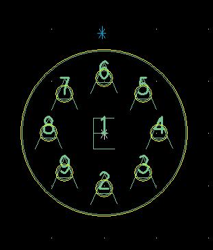
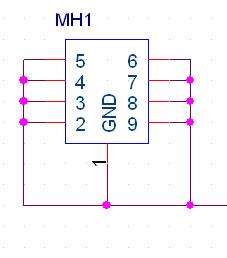
regarding the vias on mounting hole i think you can place vias on the footprint itsself as pins (refer fig.)
while doing schematic include the vias in the symbol.
you may use shapes in Top layer for the breaks shown in figure.
If it still give errors means you can waive those errors (from display-->waive DRC--> waive) and this will eroors will be trated as 'known errors'
This site uses cookies to help personalise content, tailor your experience and to keep you logged in if you register.
By continuing to use this site, you are consenting to our use of cookies.
 thank you all reply. i got idea.