Continue to Site

Welcome to EDAboard.com

Welcome to our site! EDAboard.com is an international Electronics Discussion Forum focused on EDA software, circuits, schematics, books, theory, papers, asic, pld, 8051, DSP, Network, RF, Analog Design, PCB, Service Manuals... and a whole lot more! To participate you need to register. Registration is free. Click here to register now.

FPGA PCI board with 3.3v/5v connector. How possible?

Status
Not open for further replies.

Sink0

Full Member level 6
Joined
Nov 25, 2009
Messages
390
Helped
37
Reputation
74
Reaction score
30
Trophy points
1,308
Location
Sao Paulo, Brazil
Activity points
4,186
Hi, i need to make a PCI board with a Cyclone II FPGA so i was taking a look on others board designs. I found 2 different boards, one at opencores and the second one is Dragon PCI FPGA board from knjn (https://www.knjn.com/FPGA-PCI.html). Looking at both i see that the PCI connector of both boards says that they can work with 5v and 3.3v but they do not have any voltage conversion between FPGA pins and PCI bus. How is that possible? How you can make sure that the PCI bus is going to talk at 3.3V and not at 5v?

I do not have the knjn board schematic but at the opencores one the Banks were powered with 3.3V.

Thank you!

Let me know if i was not enough clear.
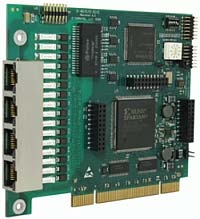
 

I think, a PCI interface with Cyclone II (or any other 3.3V limited interface chip) should not have a 5V key at the connector. This is clearly a design fault. The other question is, if you seriously have to take a system with 5V PCI (pre PCI 2.2) into acount.
 

Well let me explain my problem. I am desgning a board to use with a PC/104+. It is a standard computer but with a different layout. There are 2 reasons to me want to make my PCI BUS work at 5V. First one is that as i dont have the PC/104 on my hands yet i am building a board for a standard computer. But as i am afraid to damage de computer i am using an old one, with a 5V PCI Bus. The second reason is becouse i am still talking with the PC/104 manufacturer to find out if his board can work with linux with no problem becouse it is made for windows. If i have to chose another board it is possible that the new board's bus just can work at 5V, so i got to be ready for that problem. Do you have any solution in mind to solve this. Build a board that i could switch the BUS voltage would be the best solution but i am still looking for good voltage level translators. Do you have any IC on mind or another solution?

Let me know if i was not enough clear!

Thank you!
 

I don't have my PCI specification at hand right now, but I think that a 5V tolerant 3.3V PCI interface basically would do. Present FPGAs (either from Altera or other vendors) aren't 5 V tolerant. But there are 5V tolerant CPLD chips, e.g. Altera MAX 3000 or Lattice LC4000V series.
 

The Altera's and Xilinx PCI dev kit uses quickiswitchs to solve that problem but the resulting bus is not totaly compliant to PCI 2.2 Specs. Do you think that solution would be enough reliable? Is it possible to implement 5 20Mbps UART on a CPLD? Or should just use it as a PCI bridge to FPGA? My last option would be use a ASIC PCI bridge...
 

I was just aware of Altera AN330, discussing the busswitch operation to achieve 5V tolerance. It says, the main limitation is in not keeping the PCI impedance specification.

The said 5V tolerant CPLD have a maximum complexity of 512 logic cells. You can possibly fit a fixed baud rate 8 bit RX/TX UART to about 100 LCs, but what about the PCI interface part? This effectively can't work.
 

Well i think i am going to try the quickswitch approach for many reasons. PCI bridges are expensive, i started with FPGAs like one month ago so that would be great for learning purposes, i don't think Altera or Xilinx would sell the kits if they did not work well, i already implemented the UARTs on FPGA and they are working quite well.

Thank you for sharing your experience.

Just one last question, when should i not use PCI-clamp diodes? The Quickswitch is going to limit voltage to 3.3V. I will use the clamp diodes anyway, is that approach correct?

Thats all

Thank you!
 

If the clamp diodes are available for the respective pins, I would enable them.

I wonder, if external clamp diodes on the PCI side can help to better comply with the
spec?
 

Hmmm do you mean with a diode to VCC as it is inside the FPGA or a 3.3V zener? I was wondering same thing, but i think there are 2 main reasons:

First becouse PCI specs at section 4.4.3.4 says that is specifically a violation of this specification for expansion boards to attach any pull-up resistor or other discrete devices on the PCI sgnals anless they are placed behind a PCI-to-PCI bridge.

Other problem would be that the diodes would interfer on other boards signals. That would be much worst than quickswitchs approach.

Am i correct?
 

I am getting back to this post becouse of FvM idea of using a CPLD for PCI bus... Any idela how many LC to make a PCI to Local bus Bridge? Something like PCI 9052 from PLX? If some one ask why i do not use the PLX IC.. the answer i need a really cheap PCI board with a FPGA, and PCI 9052 would add much cost on the board, and i am still considering on buying a already made board. I cant find any cheap with a FPGA on it.. but i can find more cheaper ones with a CPLD with a PCI form.

CYa
 

Sink0 said:
Hi, i need to make a PCI board with a Cyclone II FPGA so i was taking a look on others board designs. I found 2 different boards, one at opencores and the second one is Dragon PCI FPGA board from knjn (http://www.knjn.com/FPGA-PCI.html). Looking at both i see that the PCI connector of both boards says that they can work with 5v and 3.3v but they do not have any voltage conversion between FPGA pins and PCI bus. How is that possible? How you can make sure that the PCI bus is going to talk at 3.3V and not at 5v?

I do not have the knjn board schematic but at the opencores one the Banks were powered with 3.3V.

Thank you!

Let me know if i was not enough clear.

Hello!
Place buffers between PCI connector and PCI device and you will have a universal board.
See Raggedstone1 schematic
http://www.enterpoint.co.uk/moelbryn/raggedstone1.html
for eхample. I use buffers on my PCI board without any problems.

-- Good Luck
 

Sink0 said:
What buffer IC do you guys use? IDTQS3861 + Level shifting diode?

Thank you

My list of solution for PCI buffering that I compose sometimes ago:


IDT:
1) QS34X245Q3G -32 Bit/QVSOP-80
2) QS3861PAG - 10 Bit/TSSOP-24
3) QS3384PAG - 10 Bit/TSSOP-24
3) QS32X861Q1G - 20 Bit/QSOP-48
4) QS32X384Q1G - 20 Bit/QSOP-48
5) QS3306AS1G 2 Bit/SOIC-8


Faichild:
1) FST16211MTD - 24 Bit/TSSOP-56
2) FSTD16211MTD - 24 Bit/TSSOP-56
3) FST34X2245QSPX - 32 Bit/QVSOP-80
4) NC7SZ384M5X - 1 Bit/SOT-23
4) NC7SZ384P5X - 1 Bit/SC-70
5) NC7WB3125K8X -2 Bit/US-8
6) FST3384MTC - 10 Bit/TSSOP-24


TI:
1) 74CBTD1G125DCK - 1 Bit/SC-70
2) 74CBTD1G125DBV - 1Bit/SOT-23
3) 74CBTD3306PW - 2 Bit/TSSOP-8
4) 74CBTD3306D - 2 Bit/SOIC-8
5) 74CBTD3384DGV - 10 Bit/TVSOP-24
6) 74CBTD3384DW - 10 Bit/SOIC-24
7) 74CBTD3384PW - 10 Bit/TSSOP-24


Pericom:
1) PI5C3384LE - 10 Bit/TSSOP-24
2) PI53861Q - 10 Bit/SSOP-24


PRICES from "findchips":
TI:
SN74CBTD3384PW 0.40 | 1ku
SN74CBTD16211DGGR 2.64 | 1ku
SN74CBTD3306PW 0.31 | 1ku


NXP:
CBTD3384 0.38 | 1ku
CBTD16211DGG 0.90 | 1ku
CBT3306PW 0.49 | 1ku


I select 2x CBTD3384 and 1x CBT3306PW for my design (PCI Master\Target). Both part have a internal diode.
 

Hmmm maybe you can save me!!.. I have available 10 SN74CBTD3384PW.. But they footprint it look unusable.. How you did route with it? CBTD3861 and QS3861 looks so much easier to use as the bus com from one side and go out at the other of the IC. Not at the same side as 3384. Is it possible to give me a print of you routing with these ICSs? And it is a total of 22 ports.. 10 of eac 3384 and 2 from 3306. For PCI i supose you need something like 50 ports... how you did it?

Dont you have any spare board for sell at a good price right? haha

Thank you very much!!
 

Sink0 said:
Hmmm maybe you can save me!!.. I have available 10 SN74CBTD3384PW.. But they footprint it look unusable.. How you did route with it? CBTD3861 and QS3861 looks so much easier to use as the bus com from one side and go out at the other of the IC. Not at the same side as 3384. Is it possible to give me a print of you routing with these ICSs? And it is a total of 22 ports.. 10 of eac 3384 and 2 from 3306. For PCI i supose you need something like 50 ports... how you did it?

Dont you have any spare board for sell at a good price right? haha

Thank you very much!!

Actually I use 2xCBTD16211DGG and 1xCBTD3306PW. (50 PCI signals)
List of chips I copy from my old post from other site.
I`m sorry for mistake.

See for "Ruggedstone1" board for reference schematic for PCI.
http://www.enterpoint.co.uk/raggedstone1/RAGGEDSTONE_CUSTOMER_COPY.zip
But they have a mistake with PRSNT1# and PRSNT2# PCI signals.

P.S.
My board (Bus switch chips between Xilinx and PCI riser)
8_1282374778.jpg
 

Hmm now it makes much more sense...

Yea.. they did a mistake at PRSNT1# and PRSNT2#. Is that mistake just on the schematic or they sell boars with that mistake? That is going to be a problem becouse the MOBO wont know that there is need of power...

Thank you for all you help!!
 

Status
Not open for further replies.

Part and Inventory Search

Welcome to EDABoard.com

Sponsor

Back
Top