Continue to Site

Welcome to EDAboard.com

Welcome to our site! EDAboard.com is an international Electronics Discussion Forum focused on EDA software, circuits, schematics, books, theory, papers, asic, pld, 8051, DSP, Network, RF, Analog Design, PCB, Service Manuals... and a whole lot more! To participate you need to register. Registration is free. Click here to register now.

Problem with overheating Mosfet in a flyback design

Status
Not open for further replies.

kalaianand

Advanced Member level 4
Joined
Jun 17, 2010
Messages
113
Helped
11
Reputation
22
Reaction score
10
Trophy points
1,298
Activity points
2,025
hello friends
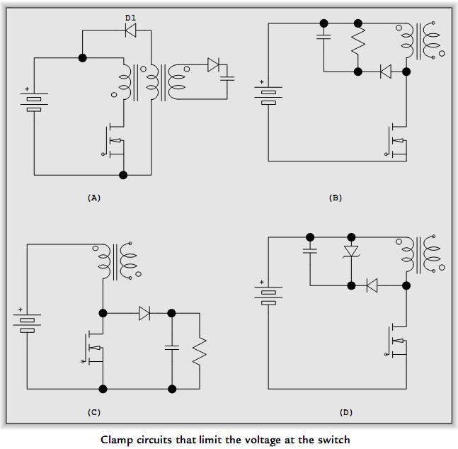
I designed one flyback circuit, whose input varies from 70-330 dc, i want to maintain output voltage constant 24V dc.At first i tested input voltage at 50v dc, output voltage is regulating. problem is Mosfet(IRFP460 500v,20A) is over heating, with in 10-15 sec, i used big size heat sink. when i measured Drain to source voltage during switching(30kHz), the voltage spikes are at magnitude more than 400V. i didnt use any snubber in my application. Is that problem due to not using snubber or some other?
If snubber is the problem, please guide me to design proper snubber circuit

thank u
 

flyback design

sounds like your FET is breaking over

u could look up "RCD snubber" for flyback.

Or diode/zener snubber for flyback

maybe powerint.com has good app note for you

or switchingpowermagazine.com
 

Re: flyback design

Hi,
Transformers and diodes have parasitic capacitances that can have undesirable consequences. The secondary capacitances, along with secondary leakage inductance, can form a high frequency resonant circuit that is excited when the diode turns off. The resonant circuit will ring and transfer the AC waveform back to the primary.
Clamp circuits (snubbers: RCD or Diode-Transzorb) are used to reduce the stress and limit maximum voltage on the switch (MOSFET/IGBT) from parasitic inductance elements.
100_1278616203.jpg


Take a look at these:
https://en.wikipedia.org/wiki/Snubber
www.cde.com/tech/design.pdf
www.hagtech.com/pdf/snubber.pdf

Hope this helps.
Tahmid.
 

Re: flyback design

hello friends
thanks for your guidance
If i use, zener-diode combination snubber circuit, how to chose zener diode rating?please suggest me for proper design.
thank u
 

flyback design

Hi,
Just for information, usually instead of zener, some similar devices known as transils or transzorbs are used. This is what you see in the above diagram as "zener".
These transils are similar to zener, in the sense that a 100V rated transil can take upto 1W or more depending on the type, BUT for a short time it can suppress and withstand very high power. A P6KE200 clips to 200V and has a short time power capacity of 600W. P15KE200 of 1500W.

I think you need to clip your voltage to around approximately 300-350V for safety of the HV MOSFET. So, here maybe you should use P6KE350 or P15KE350.

www.datasheetcatalog.org/datasheet/panjit/P6KE130CA.pdf
https://en.wikipedia.org/wiki/Transient_voltage_suppression_diode
https://en.wikipedia.org/wiki/Transient_voltage_suppressor

Hope this helps.
Tahmid.
 

    kalaianand

    Points: 2
    Helpful Answer Positive Rating
Re: flyback design

hi tahmid
i am designing snubber circuit for my flyback converter
for choosing capacior...
which type i have to choose
is Disc type capacitor with voltage rating 1000V is sufficient?
shopkeepers saying that disc capacitor is for DC. But i dont think so, .... can i use those disc capacitors in snubber?
please clarify me soon

Added after 19 minutes:

hi friends
i am designing snubber circuit for my flyback converter
for choosing capacior...
which type i have to choose
is Disc type capacitor with voltage rating 1000V is sufficient?
shopkeepers saying that disc capacitor is for DC. But i dont think so, .... can i use those disc capacitors in snubber?
please clarify me soon
 

Re: flyback design

hello friends
as i am struggling with the overshoot voltage problem, i plan to use flyback converter with two switch configuration. could u please give me suggestion that, how to genetate two gate pulse of same phase at a time. I saw some configuration which uses pulse transformers, will that work at high frequency? if so, how to designn that?
I tried with IR 2110 driver IC, but its not working properly in bootstrap configuration. remeber that i have to use one supply. i dont have isolation supply in my design.
please give me your suggestions its urgent.......
 

Status
Not open for further replies.

Similar threads

Part and Inventory Search

Welcome to EDABoard.com

Sponsor

Back
Top