steven_l
Member level 1
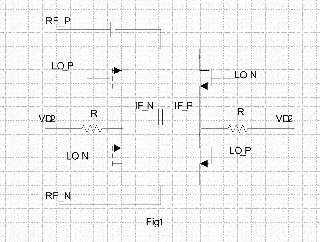
I am designing a resistive mixer which requires high linearity. So I choose resistive mixer, see Fig1.
After I finish the stimulation, I find the NF is very high, about 20dB and conversion gain is low, about -8dB. IIP3 is 16dBm and P1dB=2dBm.
I do not know how to reduce the NF and increase conversion gain.
I do not know whether my switch size and DC bias is right.
I use 0.25 tech.
And switch size is 280um/0.25u.
VG=1V
VD2=390mV.
LO power is chosen as 5dBm,which means Vrms=440mV for 50 ohm load.
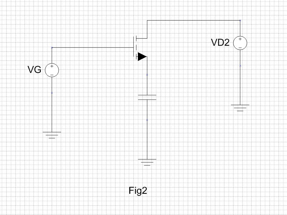
I stimulate the circuit in Fig2 by setting VG=0.9V+220mV=1.12V to see the Ron resistor or setting VG=0.9V-220mV=0.68v to see the Roff resistor.
The reason for I choose 220mV, half of Vrms-44omV, is that if LO is a sin function, V=440sin(ωt), 220 mV stands forωt=pi/6. pi/6 is a relative small part of the period. So, I think, if a switch can ON or OFF withinωt=pi/6, it will keep ON and OFF during almost of the period.
The result is when VG=0.9V+220mV, Ron=24 ohm, when VG=0.9V-220mV, Roff=6K ohm.
Of course, maybe Ron is still large and Roff is too small. I try to increase Roff and decrease Ron by setting a large size from 240um/0.25um to 300 um/0.25um. But the result is Ron=19 ohm, Roff=4.8K ohm. As we can see, Ron changes little. So just enlarge size is not a good method. On the contrary, more LO power is needed.
And the Conversion Gain changes from -8dB to -7.5B. This confuses me, because large size improves CG. However, here it reverses. I do not know why.
Oh, the noise summary shows that:
The resistor connecting to drain bias contributes the most noise, about 21.75% for each one
The second one is the switch channel resistor noise, about 13.27% for each one
Then is flicker noise of the switch, about 0.13% for each one
Any one can tell me how to reduce the R’s contribution. Or how to set the drain DC bias to reduce its noise contribution?
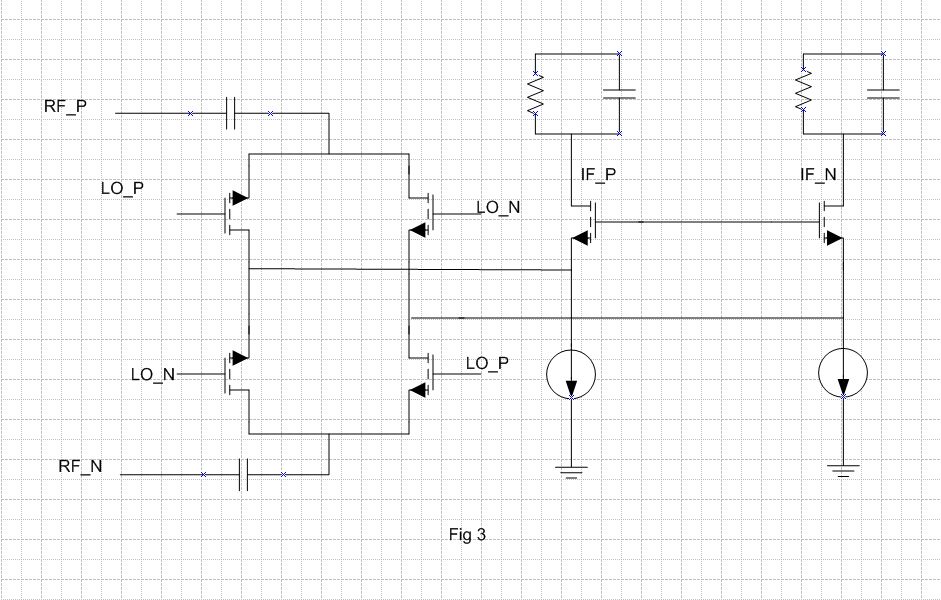
Also I have tried the circuit in Fig 3. But still NF is too large, which is mainly from the common gate transistor, the current bias and the load.
How can I do?