Continue to Site

Welcome to EDAboard.com

Welcome to our site! EDAboard.com is an international Electronics Discussion Forum focused on EDA software, circuits, schematics, books, theory, papers, asic, pld, 8051, DSP, Network, RF, Analog Design, PCB, Service Manuals... and a whole lot more! To participate you need to register. Registration is free. Click here to register now.

understand the working of the circuit, college project

Status
Not open for further replies.

neebee

Newbie level 4
Joined
Mar 15, 2010
Messages
5
Helped
0
Reputation
0
Reaction score
0
Trophy points
1,281
Location
india
Activity points
1,314
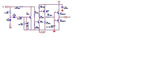
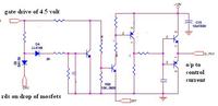
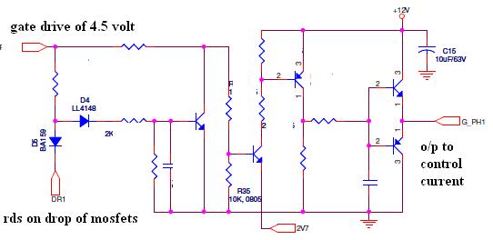
can anybody in the forum will help me out to understand the working of the circuit as i require it very badly for my college project pls. help me out if you can pls. pls. pls.


HTML:
18_1268724892.jpg

Traditional link:
https://obrazki.elektroda.pl/18_1268724892.jpg
 

working of the circuit

If you ignore D4/D5 and the first transistor it is simply a level shifting driver with push-pull emitter followers. While the connections to other circuitry are not shown, D4/D5 etc looks like it will reduce the drive based on a signal through the port DR1.

Keith.
 

Re: working of the circuit

thnx a lot for helping me but i am not that much advanced user who can understand the circuit can you help me out as i mentioned in my diagram that how it will work whenas i given the drive pulse of 4.5 v in left side and input of vds which will depend on the current drawn from mosfet in the bottom terminal than how this circuit will work when my drives are constant and only the vds will increase i want to understand the working of this circuit step by step so that i can prepare my college project pls. help me out.


HTML:
23_1269243446.jpg

Traditional link:
https://obrazki.elektroda.pl/23_1269243446.jpg


keith1200rs said:
If you ignore D4/D5 and the first transistor it is simply a level shifting driver with push-pull emitter followers. While the connections to other circuitry are not shown, D4/D5 etc looks like it will reduce the drive based on a signal through the port DR1.

Keith.
 

working of the circuit

There are no component values on the circuit and the connection of the DR1 input is not defined, so I can only generalise as to how it works.

If you label the transistors Q1 to Q5 left to right, then Q2 will turn on when the voltage on its base is above around 3.4V (2.7V plus one Vbe drop). The exact input voltage this happens at will depend on the values of the unmarked resistors.

Q3 then inverts that signal while also shifting the voltage to 12V.

Q4 & Q5 form a complementary emitter follower pair, presumably to drive the MOSFET gate.

The diodes and Q1 will progressively turn off the base drive to Q2 depending on the voltage on DR1. A high voltage on DR1 will allow Q1 to turn on which will partially short out the base drive to Q2 through the resistor divider, thereby reducing the gate drive.

Keith.
 

    neebee

    Points: 2
    Helpful Answer Positive Rating
Re: working of the circuit

thnx again for helping me out and pls. find the schematic with all the details and pls. let me know how the circuit is working stage by stage and pls.also let me know the best possible way to switch off the q2 when a voltage level is applied to dr1.
 

working of the circuit

I have already described the general operation. You can work out the various voltages from the resistor values using basic electronics knowledge. DR1 just monitors the drain voltage of the MOSFETs. When the drain voltage drops low enough it will pull down D5 which in turn will turn off Q1. Otherwise Q1 would be turned on due to R42, D4, R13.

I don't know what the circuit is designed to achieve - it appears to be trying to have a specific drain-source voltage drop, but I don't know why. Either that, or it is designed to be "unstable" and hence produce a chopping effect.

Keith.
 

Status
Not open for further replies.

Part and Inventory Search

Welcome to EDABoard.com

Sponsor

Back
Top