Continue to Site

Welcome to EDAboard.com

Welcome to our site! EDAboard.com is an international Electronics Discussion Forum focused on EDA software, circuits, schematics, books, theory, papers, asic, pld, 8051, DSP, Network, RF, Analog Design, PCB, Service Manuals... and a whole lot more! To participate you need to register. Registration is free. Click here to register now.

Frequency compensation of audio amp

Status
Not open for further replies.

fg

Junior Member level 3
Joined
Feb 2, 2010
Messages
25
Helped
1
Reputation
2
Reaction score
0
Trophy points
1,281
Location
Finland
Activity points
1,549
Hi everyone!

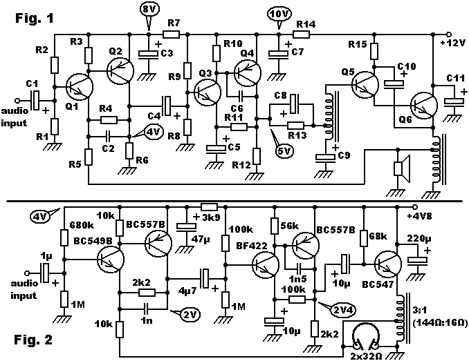
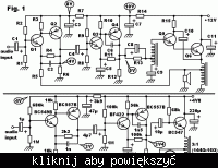
Fig. 1 shows a class A audio amplifier with transformer output. The amplifier in Fig. 2 is much similar to Fig. 1 but it drives headphones rather than a speaker and there is only one emitter follower stage and no interstage transformer, unlike in Fig. 1.

Both circuits show two frequency compensation capacitors (C2 and C6 as in Fig. 1), connected in a similar way. The latter circuit (Fig. 2) has been tested and it does not appear to oscillate except briefly upon startup (don't know why), at an audible frequency (less than 50 hertz).

A brief description of Fig. 1:

Q1 is the error amplifier. Feedback current from the amplifier's output comes to Q1's emitter via resistor R5.

Q2, Q3, and Q4 are voltage amplifier stages. The transformer in Q4's output will raise the stage's output voltage so that it can drive Q5 at a signal level of 12 volts peak-to-peak.

Q5 and Q6 are current amplifiers in common-collector configuration. Q6 drives the output transformer (a 12 ohm to 4 ohm autotransformer). C10 is a bootstrap capacitor, required so as to raise Q5's collector voltage as its base voltage rises.

Resistors R1, R2, R8, R9, R4, and R11 are for biasing the transistors Q1...Q4. R4 will also induce some degree of local feedback from Q2 to Q1.

C5 will prevent local feedback from Q4's collector to Q3's emitter. This allows for a high open-loop gain of the amplifier.

C1 couples the input of the entire amplifier. C4 and C8 are coupling capacitors between the amplifier stages. R13 will provide Q5 with bias current. C9 is intended to keep the bottom of the interstage autotransformer at a constant voltage.

R7, C3, R14, C7, and C11 will provide filtering of supply voltage. They will also isolate the amplifier stages from each other, preventing any kind of undesired feedback via the supply rails.

R3, R6, R10, and R12 are collector load resistors for Q1...Q4, respectively. R15 supplies collector current for Q5.

What I'm concerned about is frequency stability. Will the capacitors C2 & C6 shown in Fig. 1 be enough to prevent oscillation? How many compensation capacitors are required anyway in a circuit like that presented in Fig. 1? Where should the capacitors be located? Are there any formulae for calculating appropriate values for them?

Please ask for any details needed. Any help will be appreciated!
 

There is no simple formula to calculate the frequency compensation. Basically you have to analyze the loop gain and determine the phase margin at unity gain. For a simple compensation scheme, the high frequency gain roll-off should be achieved by a single dominant pole. That means one compensation capacitor rather than two. Bode plots are a usual way to visualize the loop gain frequency characteristic.https://en.wikipedia.org/wiki/Bode_plot

I can't say anything about Fig.1, because no dimensioning is given. Furthermore, the circuit can't be analyzed without knowing the transformers main and leak inductance. Assuming an ideal transformer, it shows, that circuit Fig. 2 is actually overcompensated by the 1.5 nF capacitor, resulting in about 3 kHz cut-off frequency.

Due to the multiple AC coupling, the circuit can easily become unstable at the lower cut-off frequency. The transformer plays an multiple-unknown part, it introduces a zero by it's main inductance and a pole by it's leak inductance. As an additional issue, it can get saturated by the DC bias and this way cause serious distortions.

The best way to get a understanding of these effects is to enter the circuit in SPICE simulator, e.g. LTSPICE and play around with the part dimensioning.

All-in-all, the circuit's looks to me like a reminiscence to a 60th design.
 

    fg

    Points: 2
    Helpful Answer Positive Rating
FvM said:
There is no simple formula to calculate the frequency compensation. Basically you have to analyze the loop gain and determine the phase margin at unity gain. For a simple compensation scheme, the high frequency gain roll-off should be achieved by a single dominant pole. That means one compensation capacitor rather than two. Bode plots are a usual way to visualize the loop gain frequency characteristic.https://en.wikipedia.org/wiki/Bode_plot

I can't say anything about Fig.1, because no dimensioning is given. Furthermore, the circuit can't be analyzed without knowing the transformers main and leak inductance. Assuming an ideal transformer, it shows, that circuit Fig. 2 is actually overcompensated by the 1.5 nF capacitor, resulting in about 3 kHz cut-off frequency.

Due to the multiple AC coupling, the circuit can easily become unstable at the lower cut-off frequency. The transformer plays an multiple-unknown part, it introduces a zero by it's main inductance and a pole by it's leak inductance. As an additional issue, it can get saturated by the DC bias and this way cause serious distortions.

The best way to get a understanding of these effects is to enter the circuit in SPICE simulator, e.g. LTSPICE and play around with the part dimensioning.

All-in-all, the circuit's looks to me like a reminiscence to a 60th design.
Many thanks FvM.

I tried the circuit in Fig. 2 with the 1.5 nF capacitor removed and it looks like the other capacitor alone (1 nF) is sufficient for frequency compensation. High frequency response is slightly better with the new setup.

I also found that the 68k bias resistor of the BC547 was too large-- replaced it with a 22k resistor in parallel with the 10u coupling capacitor (Fig. 2). The emitter current of the output transistor (BC547) is now pretty close to the intended 16 2/3 mA (i.e. 2.4V / 144 ohms).

Finally, the bootstrapping arrangement shown in Fig. 1 is not actually needed since the emitter voltage of Q5 will never rise above 12 volts. C10 can be removed and R15 can be omitted.

Best regards,
fg
 

Do you actually know the transformer properties (main and leak inductance, saturation current)? They would be needed for an exact circuit analysis.
 

The second circuit oscillates at 50hz during startup because the bias for the BF422 is bouncing up and down because the output transistor is causing it to jump up and down. it is positive feedback. So RC filter the bias for the BF422 transistor.
 

I think, it's rather feedback with multiple AC coupling, you can see it in a simulation. But
without knowing the transformer inductance, it's just guessing.
 

FvM said:
Do you actually know the transformer properties (main and leak inductance, saturation current)? They would be needed for an exact circuit analysis.
None known exactly about Fig. 1 but some rough values can be given for Fig. 2 (see below). The DC bias current through the output transformer in Fig. 1 is 500 mA; this is fairly much and will saturate a small transformer easily. A push-pull design with a 2x24 ohm primary winding would be able to deliver the same output power with a smaller transformer.

Audioguru said:
The second circuit oscillates at 50hz during startup because the bias for the BF422 is bouncing up and down because the output transistor is causing it to jump up and down. it is positive feedback. So RC filter the bias for the BF422 transistor.
Thanks. I tried two 47 k resistors in series with a 10 uF capacitor to earth from their junction as a replacement for the 100 k bias resistor of the BF422. It won't help, however. The oscillation (just a few hertz actually, not sine wave) only occurs when power is turned on and it stops after the voltage across the 47 uF filtering capacitor has reached a certain value.

Furthermore, any feedback via the positive supply rail from the output transistor's collector to the BF422's base will be negative feedback rather than positive. However, it seems, positive feedback may occur from the output transistor's collector to the emitter of the BC557B driving the output transistor. (Not sure.) The 220 uF filtering capacitor should theoretically prevent this.

** A correction: Any feedback from the output transistor's collector to the emitter of the mentioned BC557B will again be negative, not positive. **

The oscillation must be associated with the global feedback in some way. I disabled it by connecting the bottom of the 10 k feedback resistor to earth rather than to the secondary of the output transformer. This totally disables any oscillation but also the global feedback.

FvM said:
I think, it's rather feedback with multiple AC coupling, you can see it in a simulation. But
without knowing the transformer inductance, it's just guessing.
The primary inductance (main inductance) of the output transformer in Fig. 2 is approximately 200...300 mH (229 mH would result in the lower cutoff frequency being about 100 Hz with no DC bias applied). Assuming it's 250 mH, the secondary inductance would be 250 mH / 9 ~ 27.78 mH (according to the 9:1 impedance ratio). These results are based on very rough approximations. I have no idea about how great the leakage inductances are (some approximations can be made, though). The transformer is a laminated core transformer with small air gap. The DC bias current is about 16.67 mA (2.4 V / 144 ohms).

All in all, the amplifier in Fig. 2 has a fairly good frequency response and no oscillation problems during normal operation. As mentioned earlier, it now uses the 1 nF capacitor alone for frequency compensation; also, the 68 k bias resistor of the BC547 has been replaced with a 22 k resistor in parallel with the 10 uF coupling capacitor.

Thanks for all the help.

Regards,
fg
 

Status
Not open for further replies.

Similar threads

Part and Inventory Search

Welcome to EDABoard.com

Sponsor

Back
Top