Welcome to our site! EDAboard.com is an international Electronics Discussion Forum focused on EDA software, circuits, schematics, books, theory, papers, asic, pld, 8051, DSP, Network, RF, Analog Design, PCB, Service Manuals... and a whole lot more! To participate you need to register. Registration is free. Click here to register now.
Well using a cap between differential signals coming out of an amplifier is a way of saving cap size. due to it being differential on both sides its like having 2*cap to ground on each output.
I would need more detail about this clocking circuit to help if I can.....
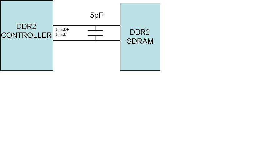
It's discussed in a micron technical note tn_47_01. They say, it can improve clock signal quality with some controller chips sets:
Figure 9 shows a capacitor placed between the clock pairs. This capacitor can improve the clock slew rates and signal quality at the DRAM. The ability of the capacitor to improve the clock signals is dependent on the clock driver. Some drivers will benefit from the addition of the capacitor more than others. Designers should check with their chipset provider to see if the capacitor the clocks is beneficial. If the capacitor is implemented place it 0.5 inches away form the first DIMM connector. The best value for the capacitor is 5pF.
It looks like a kluge that was added to improve performance between those two SPECIFIC chips. Possibly the load chip had a horrendous impedance mismatch to the driving chip, and the reflections were causing clock edge errors. Slapping on a 5 pF cap did something to move the reflections around in time so they were no longer a problem--a poor solution at best. If you relayout the board with different line lengths, the 5 pF capacitor may do more to hurt than help the situation.
It looks like a kluge that was added to improve performance between those two SPECIFIC chips. Possibly the load chip had a horrendous impedance mismatch to the driving chip.
The solution has been suggested by Micron particularly for DIMM modules. The specific situation with DIMM modulues (and
similar multi-chip designs) is that a clock partyline is feeding many chips (even if the module has two or three clock input pairs).
They can be perfectly matched with the specified 100 ohm termination resistor and still have large reflections due to the
chip input capacitances. In so far it's rather a general problem of DDR2 memory designs than a Micron specific problem. But
I completely agree, that it's not a generally recommended solution. The same application note is also discussing similar
capacitors for various single ended DDR2 control signals.
This site uses cookies to help personalise content, tailor your experience and to keep you logged in if you register.
By continuing to use this site, you are consenting to our use of cookies.
 [/
[/