Continue to Site

Welcome to EDAboard.com

Welcome to our site! EDAboard.com is an international Electronics Discussion Forum focused on EDA software, circuits, schematics, books, theory, papers, asic, pld, 8051, DSP, Network, RF, Analog Design, PCB, Service Manuals... and a whole lot more! To participate you need to register. Registration is free. Click here to register now.

CMOS relaxation oscillator Design ...

Status
Not open for further replies.

haribabu

Junior Member level 2
Joined
Jul 8, 2006
Messages
20
Helped
1
Reputation
2
Reaction score
1
Trophy points
1,283
Activity points
1,449
Hi ...
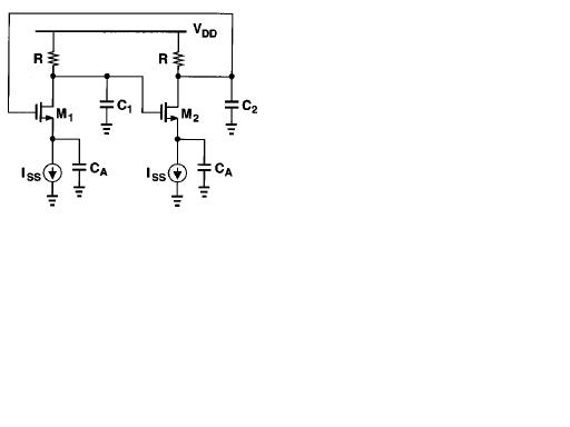
I am designing a cmos relaxation oscillator connected to a crystal . My circuit look like this ..


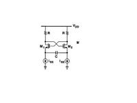
I connect the crystal working with resonance freq at 50MHz between the two outputs. The issue is, there are no oscillations produced at all .The circuit is getting latched .I measured the negative resistance at 50MHz which is around 5x times the oscillator resistance . Still i am not seeing any oscillations . Can anyone help me in understanding the concept and help me in designing this oscillator.

Thanks
Hari .
 

That doesn't look like a relaxation oscillator to me. It is DC
latch-prone especially if your load resistance is high relative
to the set-current. The current sources I believe need to
be very high effective impedance.

I think you should dig for proven crystal oscillator topologies.
Simple inverters driven linear, may be better if you are making
a digital clock and not a sine RF source.

But simulating crystal oscillators is also a bit of art in itself.
They can be tricky to start, consistently at least. If you can
see the oscillator latching / railing / stuck, though, it's probably
a topology / values problem and not just simulation issues.
 

You possibly had a two-transistor butler oscillator in mind?


Hi guyz
Thanks for taking time in giving reply.I am attaching my reference paper from which i got the above circuit .
@dick_freebird
I am looking for low power crystal oscillator circuit .I already have my inverter based crystal oscillator ckt . designed but the power consumption is huge (10mA @50MHz) .. Therefore i am trying the above ckt which claims to be low power . Please suggest me if you know any other low power architectures .
@fvm
I don't have any idea of the butler oscillator, I am looking for a MOS implementation .I will go through it and see if it finds useful for me . Thanks for your reply .


Regards
Hari .
 

Ofcourse it is a relaxation oscillator without the crystal.
If you want the oscillator to behave as a crystal oscillator slaved to the crystal frequency, you would want to kill the ability of the circuit to operte in relaxation mode.
I'm not sure that you are looking for a relaxation oscillator with a crystal connected (as your title and question comes to say)
This crystal oscillator is discussed here
 

    haribabu

    Points: 2
    Helpful Answer Positive Rating
Hi Saro ,

I am looking for a crystal oscillator behaviour and not the relaxation behaviour. Thanks for your very useful reply ... The following post is very helpful ...

I found the mistake in my ckt, which is because of using ideal current sources (derived from a current mirror ckt .) instead of biasing two tail current sources from the drains after some filtering, but i didn't get properly the concept behind the latter implementation .Would u please help me in getting that ?

Regards
Hari .
 

Hi Haribabu,
The structure that you had initially used would work but it has conflicting requirements. It needs high drain resistors to reduce the power consumption psrr, etc, but if you increase them, there would be a conflict between the tail current source and the resistors ((VDD-VCM)/R) to establish the current and can take a long time to settle. If the current source is ideal, it would prevent any swing at the drain. The common mode voltage would depend on the bias current and this also makes the CM nodes as high impedance nodes.
If you replace the resistors with current sources as it is, you can bet that the circuit would not work.

Getting the votage bias from the common mode node, defines the CMV, improves the startup greatly (This is the best starting XO I have ever seen) and allows you to use current source loads reducing supply induced jitter and area., but the current source might bring in a lot of noise too.
If you are using this structure, use the RC filter as indicated. This is to make sure that the voltage swing at the drains are filtered out. Otherwise this may get amplified and degrade the phase noise a lot.
Cheers,
Saro
 

Hi Saro,
Thanks a lot ... Ur expertise in oscillator design made my task easy . Are there any mathematical relations that help me in choosing the value like Cs ( capacitor between two source) and the filter R & C values . What happens if we directly connect gate of the bottom transistors to the drains of cross coupled pair as given in the attached file 'High Stability Low Power OSC report.pdf' and also how do we limit the amplitude of oscillations (any circuit present ) ? ..

Thanks
Hari .
 

The max limit for Cs is given in the paper.
At the operating frequency, the impedance of Cs must be much lesser than the parasitic impedances across the current sources. They form a delta connection and when it is converted to a Y-connected network, the impedance to ground must be high.
R and C are just coarsely chosen to filter the 35MHz swing. The tail current sources are supposed to be bias elements and not amplifiers. The gm of the current sources has to be kept very low if the filter is not used (which might increase the parasitics at the drain). If the filter is not used and the gm is not low enough, the swing at the drain will be impacted by the tail current source and it's noise gets amplified.
 

Hi Saro,
It has been long time since i posted this message. I have quick doubt here. Since it is a relaxation oscillator without the crystal, i want the check the Barkhausen criteria for this circuit .
Redrawing the above circuit as


i) To satisfy the phase criteria of 360° each stage has to provide 180° of phase shift. Each stage contains one left hand zero and two left hand poles.How can a left hand zero and two left hand poles give 180° phase shift ?.

ii) What is the DC closed loop gain (Positive feedback or Negative feedback) ?

Thanks
Hari.
 

Hi haribabu,

a relaxation type oscillator (it should be better called "generator", since the term "oscillator" should be reserved for sinusoidal harmonic oscillators) is NOT linear and, therefore, cannot and must not fulfill the linear oscillation criterion (Barkhausen).
It is calculated using completely different rules.
 

MODERATOR ACTION: You get a Warning!
Do not upload any IEEE copyrighted papers. You will be banned


Hi LvW,
i) If not through Barkhasuen criteria, Can u please provide me the explanation for the operation of the above circuit ?
ii)In the following paper section-VII explains it operation through Barkhasuen criteria, Please give your comments on this.
 

haribabu said:
Hi LvW,
i) If not through Barkhasuen criteria, Can u please provide me the explanation for the operation of the above circuit ?
ii)In the following paper section-VII explains it operation through Barkhasuen criteria, Please give your comments on this.

To I) General principle of a relaxation type oscillator: The output of an opamp is switched continuously between its extrems (supply voltages) caused and controlled by double feedback (positive and negative):
*positive fixed feedback factor setting a positive resp. a negative threshold; *negative feedback via an RC path with loading effect (e-function).

To II) Razavi himself gives the explanation in the first sentence of chapter Vii:

When designed to operate at 900 MHz, this circuit hardly “relaxes”
and the signals at the drain and source of and are close
to sinusoids. Thus, the linear model of Fig. 7 is a plausible
choice.


Therefore, the circuit behaves more or less "linear" and linear circuit theory (including Barkhausens rule) may be applied.

Added after 3 minutes:

Addendum: Sorry, I did not realize that you are not using an opamp. Thus, the explanation is abit different - but the general principle is quite the same.
 
  • Like
Reactions: CataM

    CataM

    Points: 2
    Helpful Answer Positive Rating
Hi LvW,
Thanks for your patient reply. I could get the operation of the relaxation oscillator. But i couldn't get how Razavi says the circuits oscillates (assuming linear model) meeting the Barkhaseun criteria with the transfer function given in the paper.It has one zero at origin and two left hand poles. How can we get phase 180° from these ?

Thanks
Hari.
 

haribabu said:
Hi LvW,
Thanks for your patient reply. I could get the operation of the relaxation oscillator. But i couldn't get how Razavi says the circuits oscillates (assuming linear model) meeting the Barkhaseun criteria with the transfer function given in the paper.It has one zero at origin and two left hand poles. How can we get phase 180° from these ?
Thanks
Hari.

The answer is in Razavi's formulation "hardly relaxes". For my opinion, he did not explain the effect in detail. However, I did not study the whole paper up to now and, therefore, cannot give a justification for his formulation. Sorry.
 

Dear haribabu,
Could you please explain to me oscillation criteria?
how to calculate Cs? and the oscillation frequency?
 

..................
Could you please explain to me oscillation criteria?
how to calculate Cs? and the oscillation frequency?

khaled, as far as I remember, Razavi spoke about a signal of app. 900 Mhz exhibiting a near-sinusoidal shape.
Thus, not only the lumped passive elements do determine the oscillation frequency but also the parasitic parameters of the active devices. Remember, these parameters are the only cause of the near-linear behaviour of the "relaxation" circuit.
Therefore, it is not easy to calculate the frequency response without knowing these transistor properties.
Hi LvW,
Thanks for your post but it does not really answer my question. If I have the values of parasitic resistances and capacitances, how can I calculate the oscillation frequency?
 

Hi LvW,
Thanks for your post but it does not really answer my question. If I have the values of parasitic resistances and capacitances, how can I calculate the oscillation frequency?

The only answer I can give you is: I couldn´t ! Too involved for deriving a formula. A typical task for a simulation program.
I think, not only parasitic caps have to be considered. At such a high frequency, also delay and storage times come into the play.
 

The only answer I can give you is: I couldn´t ! Too involved for deriving a formula. A typical task for a simulation program.
I think, not only parasitic caps have to be considered. At such a high frequency, also delay and storage times come into the play.

Hi,
It is sure for simulation tools. But designer role is to estimate roughly what is going on. At least to estimate the operating range. Otherwise most analogue books and papers are useless.
Anyway, I wounder why I feel some answers are very generic. If someone wants to help, it will be very kind from him/her. But general posts like "Many factors affect everything". "The procedure is not easy". "The oscillator design is an art itself" don't help much I am afraid.
 

Status
Not open for further replies.

Similar threads

Part and Inventory Search

Welcome to EDABoard.com

Sponsor

Back
Top