Continue to Site

Welcome to EDAboard.com

Welcome to our site! EDAboard.com is an international Electronics Discussion Forum focused on EDA software, circuits, schematics, books, theory, papers, asic, pld, 8051, DSP, Network, RF, Analog Design, PCB, Service Manuals... and a whole lot more! To participate you need to register. Registration is free. Click here to register now.

how to solve this ERC Warning in Virtuoso? (Latchup rule)

Status
Not open for further replies.

wolfrain

Junior Member level 1
Joined
Nov 14, 2009
Messages
19
Helped
1
Reputation
2
Reaction score
1
Trophy points
1,283
Location
Southampton
Activity points
1,454
At this moment, this is my first time to do the layout with Virtuoso (Cadence), and come up with a ERC Warning:

Latchup rule LAT3 distance s/d diff pgate net_welltap > 20

Does it mean I do have enough taps for the PMOS/NMOS? What should I do?

Thank you for your help. :)
 

Re: how to solve this ERC Warning in Virtuoso? (Latchup rule

wolfrain said:
Latchup rule LAT3 distance s/d diff pgate net_welltap > 20
DRC/ERC messages often are confusing, because you never know if they tell you the reason of an error, or what you should change.
In your case, I guess the distance between the s/d region and the welltap is too far.
 
Re: how to solve this ERC Warning in Virtuoso? (Latchup rule

Thank you very much for your help here. :)

I put some taps among the diff contacts and the problem is solved.

Right now I am thinking the problem of

net_psub net_subtap:Causes multiple stamped connection
net_psub net_subtap:has multiple stamped connection

and maybe the following URL might be useful:


Regards,
 
Re: how to solve this ERC Warning in Virtuoso? (Latchup rule

wolfrain said:
net_psub net_subtap:Causes multiple stamped connection
net_psub net_subtap:has multiple stamped connection

and maybe the following URL might be useful:
Yes, I hope this will help you, too!
Regards, erikl
 
Re: how to solve this ERC Warning in Virtuoso? (Latchup rule

Hello,
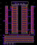
I'am also using Cadence and I have got the same problem: Latchup rule LAT3 distance s/d diff pgate net_welltap > 20. I think I have already link the PMOS with VDD and NMOS with the ground. So can you help me solve this problem? layout.jpglayout.jpglayout.jpg. Thank you advance for your response.
Best regards,
You WANG
 

I can't see the nwell region for the PMOS.
 

It's the white boundry(the two PMOS upper center)
 

The nwell must include the whole PMOS transistors. Does it?
 

Then I think the ntaps are actually too far (>20µm) from the PMOS sources. Try and insert further ntaps between the drivers and the driven PMOSes, at both sides.

You'll probably need to route all these ntap contacts by metal1, so you'll have to cross the driver wires by metal2 - or vice versa.
 

Then I think the ntaps are actually too far (>20µm) from the PMOS sources. Try and insert further ntaps between the drivers and the driven PMOSes, at both sides.

You'll probably need to route all these ntap contacts by metal1, so you'll have to cross the driver wires by metal2 - or vice versa.


In fact there is a problem of the structure. I have solved the problem.Thank you very much.
 

In fact there is a problem of the structure. I have solved the problem.

Would be nice if you explained the solution anyway, to help others not to run into the same problem.
(Even if it was a silly mistake: don't be ashamed - anybody could make the same ;-) )
 

In fact I don't really understand why, perhaps my MOS are too long. After I have changed the shape, it's ok.
 

By that you probably decreased the distance between the ntaps and the farthest source below the 20µm limit.
 

Yes, you are right, I have verified this rule。
 

Status
Not open for further replies.

Part and Inventory Search

Welcome to EDABoard.com

Sponsor

Back
Top