Continue to Site

Welcome to EDAboard.com

Welcome to our site! EDAboard.com is an international Electronics Discussion Forum focused on EDA software, circuits, schematics, books, theory, papers, asic, pld, 8051, DSP, Network, RF, Analog Design, PCB, Service Manuals... and a whole lot more! To participate you need to register. Registration is free. Click here to register now.

[help]Design issues on two stage foled cascode OTA

Status
Not open for further replies.

BackerShu

Member level 3
Joined
Dec 22, 2007
Messages
57
Helped
1
Reputation
2
Reaction score
0
Trophy points
1,286
Location
USA
Activity points
1,795
I want to design an OTA for SH circuit in Pipelined ADC and some of the important specicications are,
Vdd=1.2V
VCMI=VCMO=0.5V
Adc>96dB
GBW>400MHz
SR>300V/us
CL=Cc=5pF(for low-noise)

The two stage folded-cascode gain-boosting OTA with hybrid cascode compensation is chosen to meet the spec(the circuit woul be given in Fig6). The AC simulation shows that the DC gain is 115dB, GBW is 500MHz and the PM is 67degree.
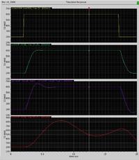
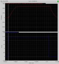
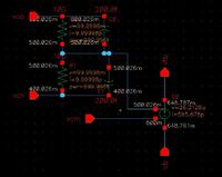
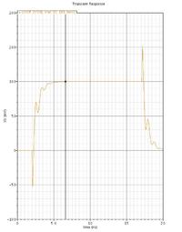
There are something about the settleing beheavior that I can't handle. Fig1~Fig4 show the settling beheavior of the OTA and Fig5 is the testbench circuit.
Fig1
[/
Fig2
[url=http://obrazki.elektroda.pl/97_1260714761.jpg][/
Fig 3
[url=http://obrazki.elektroda.pl/37_1260714837.jpg][/
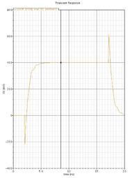
Fig 4
[url=http://obrazki.elektroda.pl/57_1260714916.jpg][/
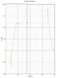
Fig 5
[url=http://obrazki.elektroda.pl/97_1260715213.jpg][/
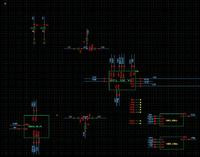
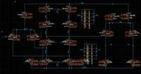
Fig 6 shows the architecture of the OTA(bias and the gain-boosting amp is omitted for simplify) and the node voltage of the DC simulation results.
[url=http://obrazki.elektroda.pl/10_1260715724.jpg][/
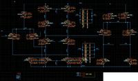
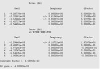
Fig 7 shows the poles/zoles of the main OTA without the gain-boosting amp
[url=http://obrazki.elektroda.pl/12_1260715935.jpg][/
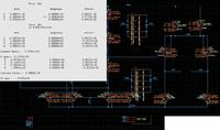
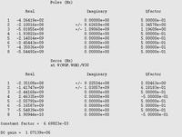
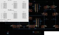
Fig 8 shows the poles/zoles of the main OTA with the gain-boosting amp
[url=http://obrazki.elektroda.pl/4_1260716026.jpg][/
these are all the pre-simulation results and I'm not sure if the settling behavior is right or if it will works when applied in Pipelined ADC. Can someone helps me to explain the settling behavior and give me some tips on how to arrange the complex poles/zoles for fast settling.
Also any comment would be appreciated.
 

You are designing fully differential amplifier, right? And you use frequency compensation technique (hybrid cascode) which corresponds to single ended amplifier. That's not correct. You have to use twice more capacitors to compensate each path from 2.
Try to fix it at the first.
 

Thanks DenisMark!
Yes it's fully differential amplifier, and the other 2 compensation you mentioned is at the right side of Fig 6 and is also omitted for simplify. I'm sorry for forgetting mentioning it in the post. So there are 4 compensate cap in the amplifier and each is 2.5pF.

the settling behavior shows that it could be settled to 14bit resolution(0.006%) in 7ns and this meet the specification. But the ring at the first part of the settling cure makes me inquietude. As Fig1~Fig4 shows, the max peak could be about 50mV. I think it may related to the complex poles/zeros shown in Fig7 and Fig8.

It seems that Fig6~Fig8 is vague in my IE broswer, but in my computer they are cleaness. I just try reuploading them here.
Fig6 the DC results of the whole OTA
[/
Fig7 the poles/zeros ditribution of the main OTA(without gain_bosting amp)
[url=http://obrazki.elektroda.pl/93_1260784056.jpg][/
Fig8 the poles/zeros ditribution of the whole OTA(with gain_bosting amp)
[url=http://obrazki.elektroda.pl/72_1260784975.jpg][/

Added after 1 hours 18 minutes:

It seems that the figures are still vague when I just use to enlarge button to see it. But if I use the URL in front of the Figures, like "http://obrazki.elektroda.pl/72_1260784975.jpg", the clearer figure appears. Is that something wrong with the way I upload the figures. I just copy and paste the BBCode with thumbnail to my post under the guideline.

Added after 4 hours 50 minutes:

for addition:
the GBW and PM of the main and two gain-boosting amp
main amp: GBW=500MHz PM=67deg
AN(in the non-signal path): GBW=550MHz PM=86deg
AP(in the signal path): GBW=520MHz PM=88deg
 

Hi BackerShu,

Some "oscillations" during transient are possible in case when roll-off -20dB/dec isn't constant before unity gain frequency (when you have some poles/zeros between dominant pole and a zero dB crossing point). If you reach straight roll-off you will improve this settling behavior. Personally I don't like pole-zero analysis because sometimes it gives abnormal results. Could you share bode plot? And how did you do AC simulations?

What's more strange are initial spikes. I guess that they are related with capacitive coupling between input pulse sources and outputs. The circuit which you used for transient response simulation isn't a conventional one (and it's hard to understand it from schematic). Why did you do so? May be feedback used by you introduces addition oscillations or instability. Usually designers use unit gain configuration with max. capacitive load (worst case of feedback).
 

    BackerShu

    Points: 2
    Helpful Answer Positive Rating
Hi DenisMark,

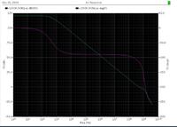
Here is the Bode plot of the AC simulation.
Fig 1
[/
And the testbench circuit is similar to Fig 2.
Fig 2
[url=http://obrazki.elektroda.pl/61_1260887720.jpg][/

As you can see, there is a terrace of the gain curve. I think it's related to the complex poles(5.02e8 +/- 1.09e9) near the GBW(500MHz). And the Qfactor of the complex poles is 1.20, I think this leads to ring? is it correct?
if so, how should I range the complex poles/zeros for this OTA?

As for transient simulation, I choose the testbench that I uploaded before for two reasons:
1) I also want to design the OTA for MDAC with close-loop gain larger than 1(such 4, for 2.5b stage), and there is no need to see the settling behavior of the OTA in unit-gain configuration. So I chose to testbench that is shown in Fig 3 to the transient behavior. I have no ideal about the oscillation introduced by this testbench, could you please elabrate it or give me some references?
Fig 3
[url=http://obrazki.elektroda.pl/44_1260887983.jpg][/

2) As for SH circuit, the feedback factor is 1 in my design and it should be test under unit-gain configuration. But I only know how to test the sigle-end opamp under unit-gain configuration. So I let input capacitor equals to the feedback capacitor to get the unit-gain configuration. As for fully differential opamp, I don't know how to set two output port in unit-gain configuration without using capacitor or Resistor as feedback components. Could please share me the testbench you used to test the transient behavior of the differential opamp?

Thanks and Regards!
BackerShu
 

Hello BackerShu,

Yes, terrace can be related with complex poles as well as with some zero. It shouldn't cause such effect because gain is below 0dB. Your Bode's plot is ok (phase and gain margins are enough).

By the way you have to improve testbenches you used. There is Cadence's whitepaper "Cadence - Functional Verification of a Differential Amplifiers.pdf" on .
Or on .
 

    BackerShu

    Points: 2
    Helpful Answer Positive Rating
Hi DenisMark,

Sorry for the late reply! I read the material you give me these two days and tried to simulate my opamp fully followed the automation testbench given by the application note, but I haven't got it yet because of my poor skill in writing script. And I will try it later, some tips from you on doing this would be appreciated.

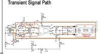
Otherwise, I improved my testbench of the OTA settling behavior test according to the note. Fig 1 shows the transient signal path of the testbench mentioned in the note.
Fig 1
[/
Since this 2 reasons,
1) there is no offset of my OTA: it's schematic simulation and I didn't introduce any mismatch to the circuit. So the "Vos feedback", as marked in Fig 1, could be omitted.
2) only the .tran simulation is done here, so the "simulation control" block could also be omitted. (I figured out that the X1 block in Fig1 is just for simulation control. Am I right? )

I changed my testbench to Fig 2
Fig 2
http://obrazki.elektroda.pl/49_1261228435_thumb.jpg[/img][/
As a result, the initial spike does disappear. But there is something new with the simulation results.
Fig 3
[url=http://obrazki.elektroda.pl/74_1261229257.jpg][/
As shown in Fig 3, from top to bottom, the first graph is the input step, the second is the differential output with feedback resistor of value 500ohm( all the four resistor are set at the same value), the third are with resistor value of 1K ohm, and the last are with resistor value of 10K ohm. I know it's because the time constant get larger with larger resistor and the results is resonable. What I confused is that the overshoot in the three graph are really different. So how could I know the exact overshoot should be because that reflect PM of the OTA, because it's related to the resistor now. Or I read the note wrong, the testbench should be further improved?

By the way, I tried substituting the OTA into the SH circuit, and the settling behavior looks resonable as shwon in Fig 4, without initial spikes, the overshoot is not too much and the settling resolution meets the spec
Fig 4
[url=http://obrazki.elektroda.pl/60_1261230270.jpg][/
Does it mean that maybe the OTA is OK and I just don't find the right way to test it? The only thing different in the SH circuit may lead the different settling behavior is real SC_CMFB. I use the ideal CMFB(Fig 5) circuit when doing the settling test. Does it have something to do with the initial spikes?
Fig 5
[url=http://obrazki.elektroda.pl/95_1261231412.jpg][/
----------------------------------------------------------------------------------
In your previous post, you said that my Bode plot is OK and the terrace won't be a problem. But some papers claimed that the terrace compelx poles/zeros would degrade the overall performance and take into the technology variation(my design is in 65nm CMOS process), the situation may be worse. So I want to push complex poles/zeros higher and make the terrace smaller or disappear. Have you any experence in designing such a OTA, some tips to do this, or some useful reference?


--BackerShu
 

Hello BackerShu.

1) Coping/Writing a script is a quite optional task for you. What's more important is to understand how to simulate different aspects of fully differential OPAMP's performance.
2) Yes, offset doesn't present in such idealized circuit especially when you don't do mismatch sims. But don't forget that offset affects on CMRR, PSRR performances.
3) Each "offset feedback" and "simulation control" isolates outputs of OPAMP from resistive feedback. It was wrong from your side to fully omit them. Because their eliminates impact of this resistive load on OPAMP performance. To be honest your OPAMP by output drivability more corresponds to OTA. You have to make such isolation and you can use VCVS elements for this.
3) When you increase resistance it looks it forms pole within input capacitance of OPAMP. You didn't isolate inputs also (and their capacitances too with "offset feedback"). You can keep them non-isolating but for simulations resistance should be less 500Ohms.
4)Spikes depends from your SH circuit.
5) Yes, terrace and associated complex poles/zeros could degrade performance when their take place >0dB or around 0dB. By your Bode's plot this terrace happpens below -6dB and your gain margin is more than 6dB as generally required. So it doesn't seem to be an issue.

Regards
 

Hi DenisMark,

Have you ever simulated open-loop gain vs vod, AC loop gain @Vod=0 and AC loop gain @vod=vod,max which were described in EE240 project?
How to add the stimulus?

Best Regards.
 

Hello HoldDreams,

I don't have EE240 under my hands but it's a quite easy.
You have to use some voltage source with DC value VOD to set differential signal and to disconnect negative feedback (for offset compensation). When you start AC simulation you will get correct circuit bias. Set desired VOD value as you want.
Also you can do AC sweep versus VOD values at some frequency of interest (very low for DC Aol).
 

DenisMark said:
Hello BackerShu.

5) Yes, terrace and associated complex poles/zeros could degrade performance when their take place >0dB or around 0dB. By your Bode's plot this terrace happpens below -6dB and your gain margin is more than 6dB as generally required. So it doesn't seem to be an issue.

Regards


Well, in fact, the gain margin is obviously no less than 5dB. And the circuit may be unstable.
 

Dear BackerShu,

Hi,
I'm working on design of a folded cascode opamp. My specifications are near of your opamp discussed here. I would appreciate it if you would kindly send me the W/L ratios or If you can't do this, tell me that are you using tsmc 180nM? I won't use them any where, without getting your permission.

Best regards,
Hesam
 

Status
Not open for further replies.

Part and Inventory Search

Welcome to EDABoard.com

Sponsor

Back
Top