Continue to Site

Welcome to EDAboard.com

Welcome to our site! EDAboard.com is an international Electronics Discussion Forum focused on EDA software, circuits, schematics, books, theory, papers, asic, pld, 8051, DSP, Network, RF, Analog Design, PCB, Service Manuals... and a whole lot more! To participate you need to register. Registration is free. Click here to register now.

help: How to analyze this schematic

Status
Not open for further replies.

master08

Newbie level 1
Joined
Nov 27, 2009
Messages
1
Helped
0
Reputation
0
Reaction score
0
Trophy points
1,281
Location
USA
Activity points
1,293
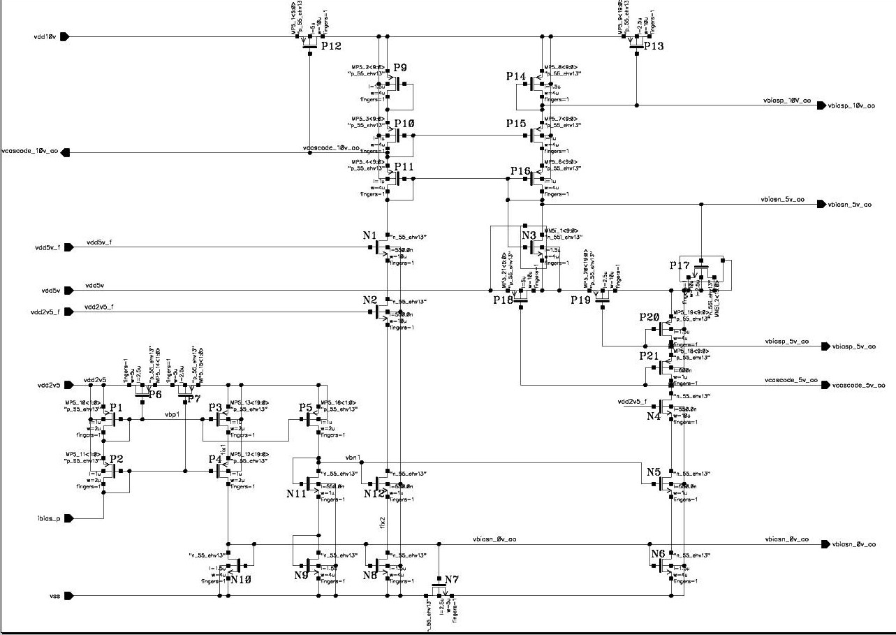
I am a freshman in this field. Now I have simulate one schematic. But I don't understand the function clearly. Please help me analyze this schematic(how about the function for every device). Thanks very much.

Question: I should remove the input pin vdd2v5(2.5v) and replace it by vdd5v.

How could I change it...
 

Break it down into pieces. Some devices are only used as capacitors. Some are only for limiting voltages and the rest is only a very simple bias and protection voltage generation circuit. It is basically what adamantiumxx told you to analyze. You can find analysis in any CMOS circuit design book.

You might want to wait until you cover this stuff in class. Freshman year you should only see sources, controlled sources, and discrete components.

Do not remove the vdd2v5. This is likely due to a drain source voltage limitation of these .5um transistors
 

Thanks for your help. I have gotten some understanding for this circuit.
 

Status
Not open for further replies.

Similar threads

Part and Inventory Search

Welcome to EDABoard.com

Sponsor

Back
Top