Continue to Site

Welcome to EDAboard.com

Welcome to our site! EDAboard.com is an international Electronics Discussion Forum focused on EDA software, circuits, schematics, books, theory, papers, asic, pld, 8051, DSP, Network, RF, Analog Design, PCB, Service Manuals... and a whole lot more! To participate you need to register. Registration is free. Click here to register now.

Cadence PCB Editor output file generation

Status
Not open for further replies.

rashdriver

Newbie level 5
Joined
Sep 7, 2009
Messages
9
Helped
0
Reputation
0
Reaction score
0
Trophy points
1,281
Location
india
Activity points
1,351
pcb assembly manufacturer

Dear Friends,

I am new for PCB Editor. I designed a PCB for some project and cross checked the dimension. For conformation i want to make that PCB physically and test the board.

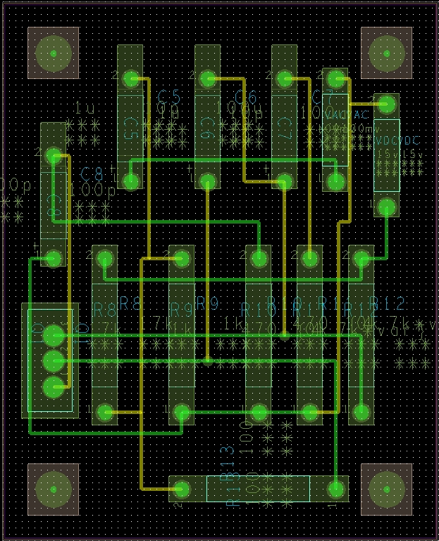
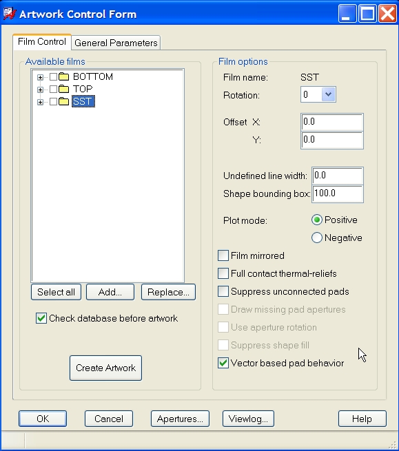
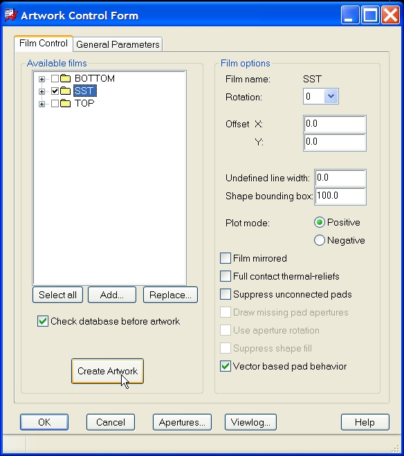
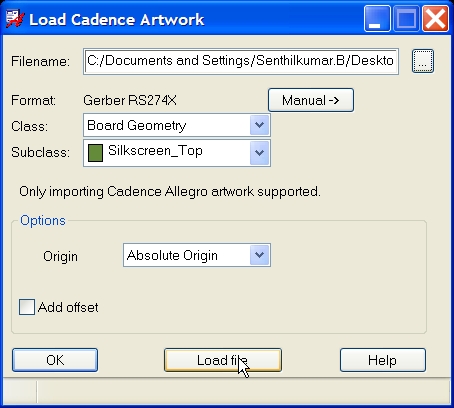
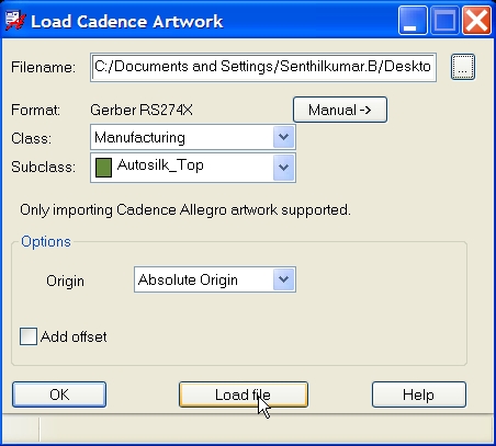
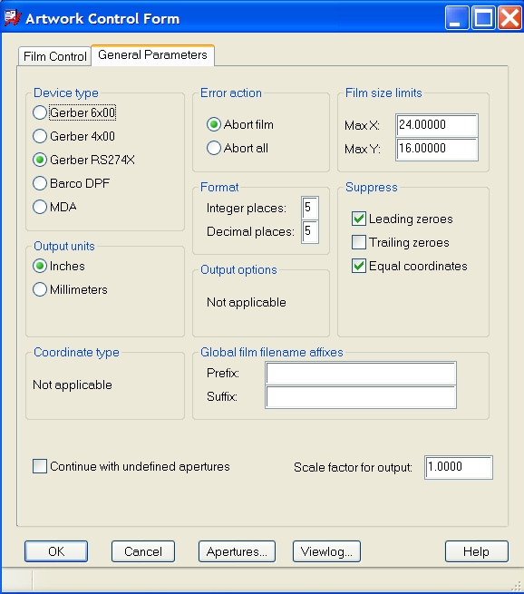
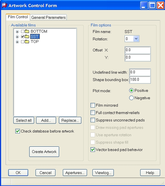
Now i created artwork files for conducting layers.

subclass creation, Display match for conducting layer profile then artwork generation.

Now the .art files generated for conducting layers. can i give these files to PCB manufacturer? if no, then what process i should do to get useful file for PCB manufacturing?

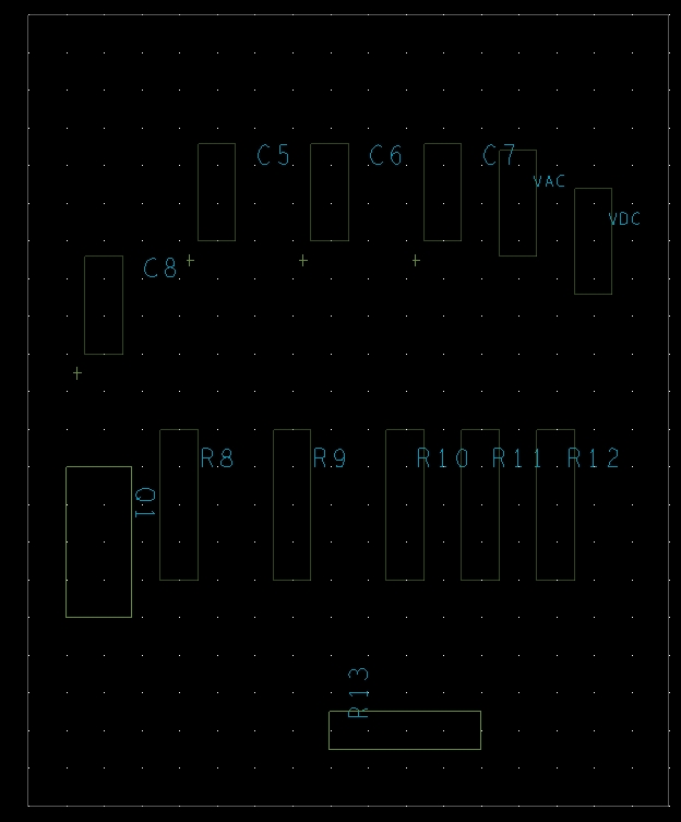
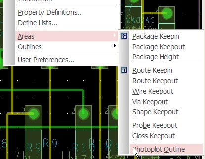
But i dont know how to create mask film, silkscreen film and assembly layout film.

If you give the remaining artwork process with some example 'such as solder mask for avoid soldering in some pads during wave soldering process' that is greatfull for knowing new things and refreshment also.

Kindly help me.

Thanks a lot for all experts.
 

First Yes .art files from Allegro are gerber files.
Second. To create a new gerber in Manufacture -> artwork right click at one entry and choose add, now give it Your wanted name eg silk-top (no funny chars here).
Then You take the colour palette and choose all off, and now select from refdes the silk top, from package geometry and from board geometry, press ok to return to artwork window, now at Your new line (silk-top) right click and choose "match display".

Thats it.

Little hint. When done in the artwork window, click select all, right click at one line (does not matter witch one). Now click at "save all selected", this will create a FILMSETUP.txt in Your working directory, use this as a template for further jobs.
Second hint. Don't know if it fixed, but earlier when doing changes in artwork window, then on leaving ever first task to do is to go to file menu and click at save, NOT at the icon and NOT save as, otherwise You might as we experience that some last changes in artwork window disappears :-(.
 

Sorry for delay. i tightly engaged with official work.

Dear lhademmor,

i tried to follow these sequence but failed to generate SST file. i cannot able to realize where i did mistake.

here i provide the snaps for these process.


This is the board design with top and bottom layer.


After visibility controlling.


creation of SST


Match display with SST


Artwork generation for SST

43_1254313343.jpg


Viewing Artwork file(SST) method1

35_1254313384.jpg


Viewing Artwork file(SST) method1 Result

40_1254313411.jpg


Viewing Artwork file(SST) method2

86_1254313446.jpg


Viewing Artwork file(SST) method2 Result


I dont know weather I cannot able to view or create artwork file.

Kindly direct me to create and viewing artwork files.

Thank you.
 

It appears that you have not set the undefined line width parameter.

Set the un-defined line width value to > 8mil i.e. say 10 mil.

Check whether your apertures are ok. For that click on apertures --> Edit --> Select apertures without rotation. then click ok.

Ensure that you select RS274X option before generating the gerber files. Then generate the art work layers.

I guess that the tool is unable to read the apertures of your .art file. this could be the reason for not being able to load/ read the artwork file into the Allegro tool.

Setting un-defined line width and setting the apertures right could solve your issue.

Added after 3 minutes:

Also try opening the .art file using a free gerber viewer tool like GC Prevue or View Mate. This should tell you whether your artwork layer is generated correctly or whether it is a problem with the tool.

Just check one more thing....check whether you have specified the photoplot outline boundary for your layout. If not, then draw the photoplot outline boundary and then generate the artwork layer.......

I think I have given u all the pointers.
 

Hi,
Thanks a lot for your reply.

I did the things upto my knowledge. kindly correct the mistakes and guide me for unknown things.

I configured device type as Gerber RS274X.


I defined the photoplot outline similar to board outline.

89_1254565250.jpg


I tried to configure apertures without rotation but failed.
In artwork control form Use aperture rotation is disabled in default.


while click on aperture icon, edit aperture window appears. Here i tyr to perform edit option.

66_1254565695.jpg


There is nothing identified for edit.


I cannot able to identify where 'un-defined line width value ' declare.

Due to these difficulty, icannot able to follow your instruction.

Kindly guide me.

Thank you.
 

Till now iam not able to generate sucessfuly.
Kindly help me.

Thanks
 

Send me the board file and ill try look at it and after then tell You where You fall into the deep :).

I cannot view the pictures with artwork output, and my guess is it is here You fall, as another person stated. Or and many do forget. Global shape setting is set to 6.00 gerber output.

BRGD klavs @ rommedahl . dk
 

Dear sir,

I am very thankfull for your valuable help.

Kindly check my design configuration and direct me to get Silk screen, Paste mask and solder mask gerbers.

File path:Demo/PCB/Allegro/Demo.brd


Find the design file from here as well as mentioned mail ID.


Thanks with Regards,
Rashdriver.
 

:-( cannot download due to, to many downloads :).
Post to e-mail stated earlier.
 

Dear everybody,

Any one help me to solve the issue please.

Rashdriver
 

You will have Your mail a litt´le latter this week. My nose did put me down for more than 10 days :-(.

I have done some screenshuts, that might help You next time as well :).

But all this neer the end of week.
 

How can i draw the arc with specific arc length?

thanks for your reply
 

Hi.

The settings in the shape menu, you have "global dynamic parameters", here You have gerber file setup as well as in the artwork tool.

15_1257528514.jpg


In the artwork tool You should state the type of gerber equal to what stated in the gdp window.

see artwork pictures.
 
Hi ,
my self Hanumagouda Patil,I am facing problem during manual routing, is there any rules to be carried out during manual routing? if so, can u please tell me the same?
My email id: hani.gmit@gmail.com
 

Status
Not open for further replies.

Part and Inventory Search

Welcome to EDABoard.com

Sponsor

Back
Top