Welcome to our site! EDAboard.com is an international Electronics Discussion Forum focused on EDA software, circuits, schematics, books, theory, papers, asic, pld, 8051, DSP, Network, RF, Analog Design, PCB, Service Manuals... and a whole lot more! To participate you need to register. Registration is free. Click here to register now.
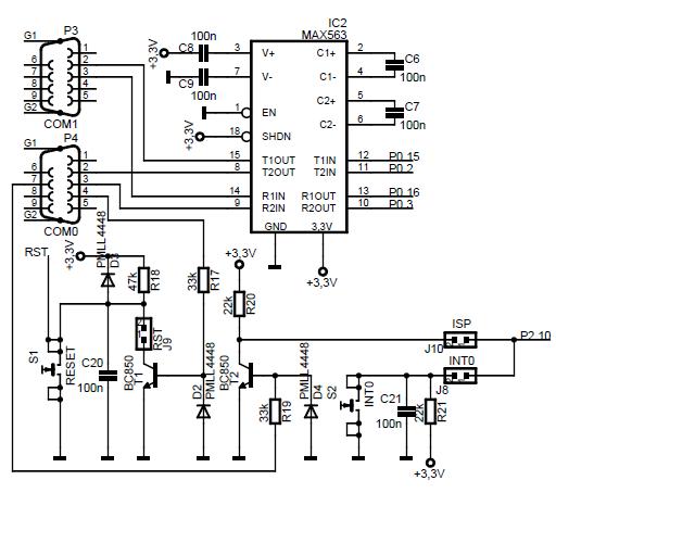
the diodes are used for the protection of the transistors
so the voltage will always be in the intended direction and if the voltage polarity reversed it will protect the circuit
The connector belogs to A rs562 562 connection that means the voltage in the wires can be negative. D2 and D4 have the pourpose of clamping the negative part of the signal.
D1 is connected to a reset circuit that is generated discharging C20 while pushing S1. If the 3.3V power supply drops, che capacitor C20 discharges through D1 generating reset
This site uses cookies to help personalise content, tailor your experience and to keep you logged in if you register.
By continuing to use this site, you are consenting to our use of cookies.