Continue to Site

Welcome to EDAboard.com

Welcome to our site! EDAboard.com is an international Electronics Discussion Forum focused on EDA software, circuits, schematics, books, theory, papers, asic, pld, 8051, DSP, Network, RF, Analog Design, PCB, Service Manuals... and a whole lot more! To participate you need to register. Registration is free. Click here to register now.

Depletion-Load nMOS Inverter

Status
Not open for further replies.

kingmaker

Junior Member level 2
Joined
Apr 3, 2008
Messages
22
Helped
0
Reputation
0
Reaction score
0
Trophy points
1,281
Activity points
1,429
nmos inverter

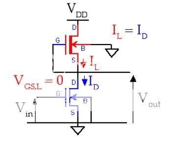
For inverter circuit with depletion type nMOS load, the gate and the source nodes of the load transistor are connected, hence Vgs(load) = 0 always? why is 0 ? anyone can explain it?

load.jpg
 

depletion load nmos inverter

In a depletion-mode nMOS the channel area is doped so that the channel exists even with no (positive) applied Vgs. Thus, the threshold of a depletion-mode is typically negative. The short-circuit between Gate and Source (i.e. Vgs=0) ensures that the transistor is always on since:
VT<0,Vgs=0
-VT>0,Vgs=0
Vgs-VT>0
 

nmos inverter

Hi,

Just in this context......

Does anyone have the book of Sung-Mo Kang, Leblebici on CMOS digital Integrated Circuits.....

Any Rapidshare link, or anything is acceptable.......
 

Status
Not open for further replies.

Part and Inventory Search

Welcome to EDABoard.com

Sponsor

Back
Top