fanrourou
Junior Member level 3
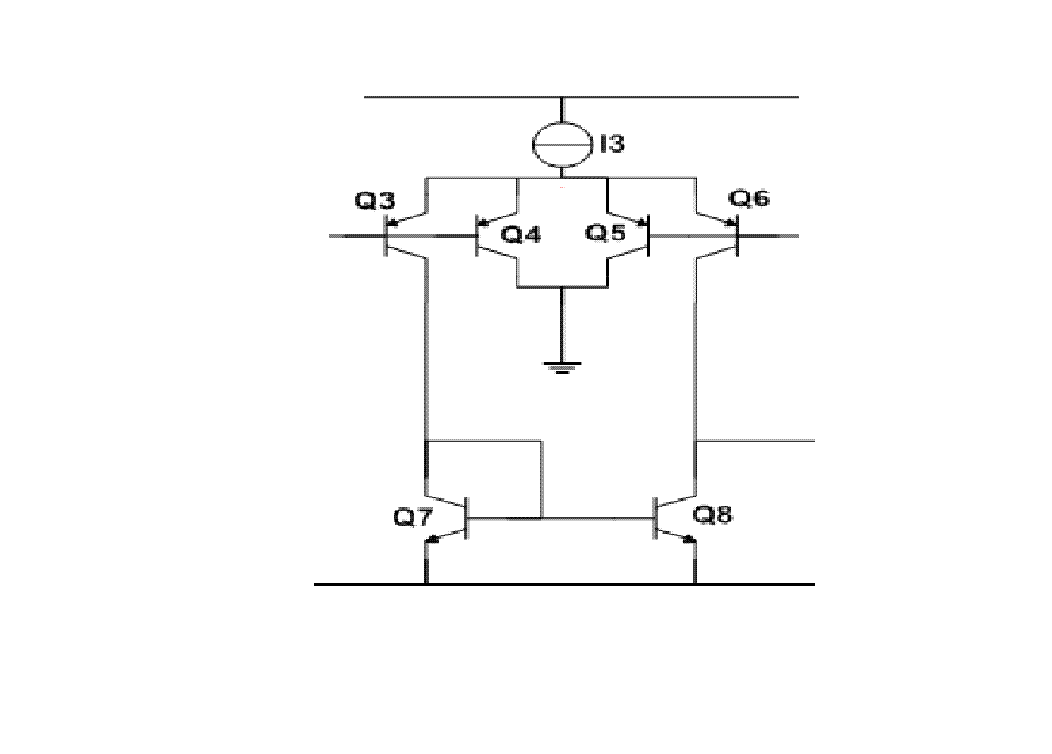
It is said that , decreasing the transconductance of input stage will increase the
slew rate of opAmp. So there is the structure shown in the picture. Q3-Q6 are
in fact one split collector lateral pnp. By setting the collector area ration of Q3-
Q6 to be 1:3:1:3, the collector currents and transconductance of Q3 and Q6
are decreased 3/4.
The question is , in my opinion, only 1/4 of the current of current source I3
can be feed to the compensation cap during the slew process. So there is
no increase in slew rate .
I just can not see how the current of I3 is all used to charge or discharge the cap !
Added after 1 hours 9 minutes:
Is it the parastic transistor will make the collector current of Q3 or Q6 equal to
I3 ?