Continue to Site

Welcome to EDAboard.com

Welcome to our site! EDAboard.com is an international Electronics Discussion Forum focused on EDA software, circuits, schematics, books, theory, papers, asic, pld, 8051, DSP, Network, RF, Analog Design, PCB, Service Manuals... and a whole lot more! To participate you need to register. Registration is free. Click here to register now.

AC Mains mosfet switch

Status
Not open for further replies.

eem2am

Banned
Joined
Jun 22, 2008
Messages
1,179
Helped
37
Reputation
74
Reaction score
24
Trophy points
1,318
Activity points
0
capacitor inrush mosfet

hello,

do you think my 2 MOSFET AC switch is OK?

it is for switch out inrush resistor in SMPS...

3166kb9.jpg
 

switching ac with mosfet

What are you doing?

You can use your mosfet switch to limit the inrush current. Look up mosfet transconductance, for a given Vgs a mosfet will allow a certain Ids.

The reason there is an inrush is because when you first flip the switch to your SMPS the bulk input capacitor is discharged the inrush current is the capacitor charging current. So adding impedance before the input cap will limit the inrush.

If all you are trying to do is some form of active inrush limiting and wish to use mosfets the simplest method is to use a photovoltaic driver.Stick your N-channel fet in between the bridge and the bulk input cap.You then have to play with the drive of the photovoltaic driver (this determines the rise time of your gate signal) which determines the maximum amount of current the fet will pass.

I've done this before and taking the measurements wont be simple unless you are in a fully equipped lab with isolated test equipment and good current probes.

The worst case inrush occurs when the switch is flipped at high line at the peak of the sine wave and the caps are all fully discharged. How are you planning to reproduce this repetitively to verify your inrush limiter is working effectively? The photovoltaic driver capabilities also varies with temperature how are you going to compensate for that?

What is the power supply that has you so concerned about inrush 500W+?

If this is just some low power SMPS just use a low value resistor in series like these

Code:
http://www.yageo.com/pdf/yageo/Leaded-R_RSF_2008.pdf
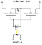
 

the connection from your gate drive ckt to the source of Q2 is wrong, Q2 should have its drain and source swapped and the gate drive connection go to the source of Q1, so that both mosfets are turned on when gate drive is applied. THe mosfets or igbts used would need to be high current types as fluctuations in the mains can give rise to high peak currents in the mosfets.
Regards, Orson Cart
 
Last edited:

I do not understand, who can explain to me.
help me. thanks.

**broken link removed**
 

I do not understand, who can explain to me.
help me. thanks.

**broken link removed**

In which part you want explanation?
The simplified circuit of the above schematic is a resistor in series with the load to limit the inrush current
and after a small delay that resistor is shorted by a switch (solid state in this case) so that the circuit works as normal.

Alex
 

Status
Not open for further replies.

Similar threads

Part and Inventory Search

Welcome to EDABoard.com

Sponsor

Back
Top