Continue to Site

Welcome to EDAboard.com

Welcome to our site! EDAboard.com is an international Electronics Discussion Forum focused on EDA software, circuits, schematics, books, theory, papers, asic, pld, 8051, DSP, Network, RF, Analog Design, PCB, Service Manuals... and a whole lot more! To participate you need to register. Registration is free. Click here to register now.

Can inductance in the gate circuit cause a negative resistance at the source terminal

Status
Not open for further replies.

Fractional-N

Full Member level 1
Joined
Oct 15, 2007
Messages
97
Helped
2
Reputation
4
Reaction score
2
Trophy points
1,288
Activity points
2,071
negative resistance

89_1219218716.jpg

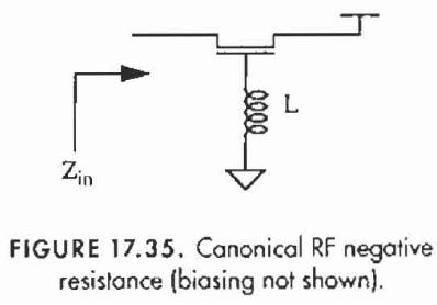
image from the design of cmos rf integrated circuits-2nd ed (Cambridge, Lee, 2004) page 642

inductance in the gate circuit of a common-gate device can cause a negative resistance to appear at the source terminal

how you prove that? (how you show that?)
 

negative resistance

Theorotical:
Convert S parameter in to Z parameters.
Add XL that is inductance to Z parameters
Again convert to S parameters.
If your S11 is >1 means you have obtained negative resistance.
You find the details about the explanations in following books
You can tally this using S11 equation. (zin-zo/zin+zo)
1) Microwave transistor amplifiers by gonzalez
2) microwave devices & circuits by Lio PHI publication

If you want to see this practically
Use simulators such as ADS
there you can directly check using tools
 

    Fractional-N

    Points: 2
    Helpful Answer Positive Rating
Re: negative resistance

Here is an attempt for an obvious and evident explanation of the effect:

A negative resistance can be thought of a voltage controlled current source which drives a current back into the voltage source.
In the circuit shown this can happen when a voltage at the source pin drives a current into the FET which causes a small current through the GS capacitance and the inductance between gate and ground (for rather high frequencies).
As a result, a voltage is created across the inductance which in turn causes a drain current (normal FET operation) which goes into the voltage source at the source pin. Thus, for a certain frequency range this circuit has a negative input resistance at the source pin.
 

    Fractional-N

    Points: 2
    Helpful Answer Positive Rating
negative resistance

Or you can consider this structure as a three port device. When you calculate 3 port s-parameters by adding a reflection coefficient at third port ( see Solid State Radio Design-I.Bahl, Prakesh et al.) you'll see S11>1 that is equivalent to negative impedance..
 

    Fractional-N

    Points: 2
    Helpful Answer Positive Rating
Status
Not open for further replies.

Part and Inventory Search

Welcome to EDABoard.com

Sponsor

Back
Top