Continue to Site

Welcome to EDAboard.com

Welcome to our site! EDAboard.com is an international Electronics Discussion Forum focused on EDA software, circuits, schematics, books, theory, papers, asic, pld, 8051, DSP, Network, RF, Analog Design, PCB, Service Manuals... and a whole lot more! To participate you need to register. Registration is free. Click here to register now.

help me please(circuit analysis)

Status
Not open for further replies.

potatoe

Newbie level 6
Joined
Jun 16, 2008
Messages
13
Helped
0
Reputation
0
Reaction score
0
Trophy points
1,281
Activity points
1,368
how many Vo of this circuit ? when switch open and closed for initial Vo =0 Volts.help explain the step for get come to which the answer of this circuit,please.
 

here is my try....

Initially let us assume that the AND gate is a TTL IC....and the capacitot is not charged...

Now when u turn on the supply(not the input)...the AND gate get it and since we assumed the IC to be TTL all open inputs are assumed to be logic 1...

so the capacitor charges to approx +5V...with its lower plate +ve...
Now u turn on the input....+12V...
this is applied to the input1 of AND gate...and due to the already available output of AND gate i.e logic 1...the output is still logic 1....this means with the application of input the state remain logic 1....

Now u close the switch...
The input gets bypassed to gnd...making input 1==logic 0 so the output of AND is logic 0...

Now the capacitor will discharge to gnd and be held at 0 Volts....the input battery wont charge teh capacitor as current will the least resistance path...i.e the gnd...

i hope this is helpful..
 

Hi,
jaywant007, a reasonable analysis of a hypothetical circuit that no one should ever try building . I guess that it is meant to be some sort of a timer circuit, or is potatoe just having a good laugh. :D
Putting 12V on the input of a TTL IC is not a good idea, using the back leakage from an input to charge a big electrolytic capacitor is not a good idea either, it would not give a reliable charge up time as it is likely to be both device and temperature dependant. The only common logic family that can still be run safely on 12V is the 4000 series CMOS and as pointed out by the previous correspondent only a TTL family device would do anything at all in this configuration apart from read 0V at the output of the AND gate (presumably where Vo is suposed to be?)and the fact that TTL will do anthing is due to a a quirk of their internal design. Never do a design that does not rely on established principles of electronics, you may get it to to work once but the next time it is built it probably won't work, also never leave a logic gate without a proper reference level and if hte input changes slowly always use a schmitt input gate or horrible things can happen when the slow voltage ramp passes through the threshold region.

Best regards,
Bob
 

1. to AdvaRes Vo mean "Voltage output".
2.to all ,sorry from my mistake that show in this picture ,actually logic gate must be NAND not AND .New picture shown below.
https://www.temppic.com/img.php?16-06-2008:1213613729_0.03144400.jpg

[size=2][color=#999999]Added after 34 seconds:[/color][/size]

picture
 

Hi,
Change the pull up voltage to 5V and the gate to a schmitt input NAND and you should have a squarewave oscillator with SW1 to disable it. The exact frequency that it oscillates depends on the threshold of the schmitt NAND gate, the 100uF and the 20K resistor.
Regards,
Bob
 

dear, DrBob13
if the pull up voltage is 12V and gate is NAND not schmitt according the picture .what's the Vo should be? help me please.
Thanks.
 

point of Vo is output of NAND ,it connected to the feedback system.
 

The value of the 20k resistor is for a Cmos NAND gate and will not work for the very high input current needed for a TTL 7400 gate.

I agree that the gate should be a Schmitt Trigger. A Cmos Scmitt Trigger NAND is a CD4093. Then the circuit is a gated oscillator.
 

Thank you for all suggestion.
To Audioguru ,I wanted to know if the NAND of this circuit(my circuit) is TTL gate ,what is happened?and if the NAND is CMOS gate(not schmitt trigger),wht is happened?
 

potatoe said:
Thank you for all suggestion.
To Audioguru ,I wanted to know if the NAND of this circuit(my circuit) is TTL gate ,what is happened?and if the NAND is CMOS gate(not schmitt trigger),wht is happened?
An ordinary NAND gate will not oscillate. The circuit's oscillator must use a Schmitt trigger gate.

The input current of a TTL gate is very high so the 20k resistor's value must be reduced to about 120 ohms. The input current of a Cmos gate is zero so nearly any resistor value can be used.

TTL needs a regulated 5V supply at a fairly high current. Cmos operates with a supply from 3V to 18V at a very low current.
 

if the CMOS gate not oscillate,how is its result should be?
Thanks.
 

potatoe said:
if the CMOS gate not oscillate,how is its result should be?
Thanks.
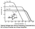
If the Cmos NAND gate's input is high then the gate will be activated and the 20k resistor will be negative feedback and its output will be at half the supply voltage.
If the input is low then the oyput will be high.
 

1.When input is high,why output is half to supply voltage ? can you make me clearly,please?
2.If NAND is TTL gate the output should be?
Thanks.
 

potatoe said:
1.When input is high,why output is half to supply voltage ? can you make me clearly,please?
Because then the gate becomes a linear amplifier and the 20k resistor from its output biases its active input with negative feedback at its switching voltage that is about half the supply voltage. See my attachment for an amplifier made from a Cmos linear logic inverter.

2.If NAND is TTL gate the output should be?
The max input current for a 74xx gate is 1.6mA and its low voltage must be less than 0.8V. A 500 ohm resistor to ground with the 1.6ma gate's input current in it has a voltage of 0.8V so the input will barely be at a logic low voltage.

The 20k resistor has a value that is way too high for the high input current of a TTL gate so the gate's input will always be high. If the other input is high then the output is low. If the other input is low then the output is high. The gate becomes a simple logic inverter.
 

Attachments

  • cmos_amp_1095.png
    cmos_amp_1095.png
    18.6 KB · Views: 184

To AudioGuRu
1.The characteristic of CMOS NAND gate will similar with CMOS inverter?
2.In regularly TTL have supply voltage 5volts .Could the input voltage of 12 volts affect with the TTL gate?
 

Hi Potatoe,
You should look at the datasheets for a CD4069 inverter and a CD4011 logic gate. They have exactly the same spec's.

You should look at the datasheet for any 74xx TTL inverter or gate. Its max allowed input voltage is much less than 12V.
 

If the NAND gate is TTL and input voltage higher than 5V it can't work properly and the gate will take damaged ?
I would be appreciate you to help me.
potatoe.
[/quote]
 

Didn't you look on the datasheet for an SN7400 TTL NAND gate?
Its max allowed input voltage is 5.5V. They do not say what happens if the input voltage is higher.
 

Status
Not open for further replies.

Similar threads

Part and Inventory Search

Welcome to EDABoard.com

Sponsor

Back
Top