Continue to Site

Welcome to EDAboard.com

Welcome to our site! EDAboard.com is an international Electronics Discussion Forum focused on EDA software, circuits, schematics, books, theory, papers, asic, pld, 8051, DSP, Network, RF, Analog Design, PCB, Service Manuals... and a whole lot more! To participate you need to register. Registration is free. Click here to register now.

question about pmos differential amplifier in a comparator

Status
Not open for further replies.

rivendu

Junior Member level 3
Joined
Dec 14, 2007
Messages
25
Helped
0
Reputation
0
Reaction score
0
Trophy points
1,281
Activity points
1,495
hi,

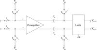
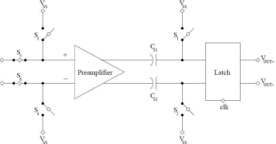
i would like to build a comparator in Output offset storage scheme like depicted below:


As the preamplifier, i want to use the differential amplifier with pmos inputs to avoid body effect.


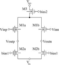
I have a problem in dimensioning the amplifier in such a way to have it working between 0V and VDD-V_saturation. The problem is related to the grounded switches. Is it a better method to connect the switches to VDD instead of ground?
How about the setting of the bias1 and bias2 voltages. Can bias1 be set to 1 and bias2 to 0 to have maximum current flowing for higher frequencies?

thanks
 

Re: question about pmos differential amplifier in a comparat

The problem is that you're using active loads (the NMOS loads). These NMOSs function as current sources. So, M2a+M2b should be exactly equal to M3 current, else the current difference will flow through the high output resistance of the current sources causing high voltage drop driving one of the transistors into triode. This requires a common mode feedback (CMFB) circuit to bias either M3 or M2a and M2b. One way for the CMFB circuit is to connect 2 large equal resistors in series between Voutp and Voutn and connect the node between the 2 resistors at one input of an amplifier and the other input to the required common mode voltage for voutp and voutn and use the output of the error amp to bias M2a and M2b (or M3) (just make sure that the polarity makes negative feedback).

Concerning the switches, if you connect them to vdd, your PMOS pair won't work because it requires Vsg=Vth+Veff.
 

hi,
regarding to the formula

A=sqrt(gm_M1a/gm_M2a) which is the gain of the amplifier, i think that M2a and M2b should be in triode region to have maximum gain, isn't it so?

Because i cannot use resistors, i should design M2a, M2b and M3 in such a way to have equal current. Do you know a method? It sounds challenging. Are there other methods without using a resistor to make this amplifier working?

When i put this amplifier into the IOS scheme (capacitors at the preamp input), the amplifier works when i set M3 into saturation and M2a+M2b into triode region by their corresponding bias voltages.

thanks
 

Re: question about pmos differential amplifier in a comparat

To achieve maximum gain, your loads should be operating at saturation not in triode. The MOS transistors have higher output resistance at saturation than at triode. For different methods for biasing the load NMOS, you can refer to "design of CMOS integrated circuits" by Razavi, chapter 9 section 9.6.
 

thanks for the link. i read this chapter but the techniques they use have too high effort. if i make the difference between the currents of M3 and M2a+M2b as low as possible, then i should have a correct functioning amplifier. another problem is the latch comparator at the output. since the capacitors block the dc signal and the latch has nmos inputs, they cannot operate in saturation region. Thus, i have to shift the output voltages of the capacitors up to V>V_nmos_sat. Is it a good choice to switch an other preamplifer at the output of the capacitors?
 

Hi,
If you do not want to use resistor, you can use the CMFB method of "CMOS Circuit Design, Layout, and Simulation" by Baker, chapter 25, 25.3.1.
And about the operate region of the NMOS input of the latch, I think you should not warry about it. You should add the Common voltage (such as Vdd/2) to instead of the Vss of the latch input node, and the AC singal of the amplifier output will be added to the Common DC voltage, so the NMOS will work in saturation region.


Best regards!
 

Status
Not open for further replies.

Part and Inventory Search

Welcome to EDABoard.com

Sponsor

Back
Top