Continue to Site

Welcome to EDAboard.com

Welcome to our site! EDAboard.com is an international Electronics Discussion Forum focused on EDA software, circuits, schematics, books, theory, papers, asic, pld, 8051, DSP, Network, RF, Analog Design, PCB, Service Manuals... and a whole lot more! To participate you need to register. Registration is free. Click here to register now.

Ultrasonic Range Finder in VHDL..plz help

Status
Not open for further replies.

greprac

Newbie level 4
Joined
Nov 8, 2006
Messages
6
Helped
0
Reputation
0
Reaction score
0
Trophy points
1,281
Activity points
1,314
Hi frendz I need to design an Ultrasonic range finder.
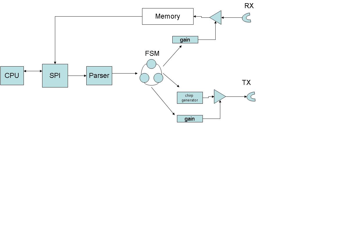
Plz help as i am an amateur wid VHDL. I am uploading the diagram and for more information plz ask me. Also it doesnt have to be very complicated.

72_1162973027.JPG
 

Frendz dont anybdy has clue abt this project???
 

I dont see hjere rationality of using fpga here as your drawigs look like data aquisition device. Are you about asic ? Or is it student project ?
 

FPGAs can be used for the memory interface and state machine design. Also, SPI, tx and rx interfaces can also be included inside FPGA. so, you just need three major chips for this project: CPU, FPGA and MEM.

Anything more specific?
 

yet add front end , time varable gain , output stage , dac, adc . I guess author is doing serious project . If not i would advice him to Devantech's SRF toys for reference design.
 

No I dont have to put it on FPGA....jus code this in VHDL...but am nt getting how to design a chirp generator and FSM. the description for FSM is as follow


Create a State Machine that interprets the commands from the CPU as follows:

command 1: START.
The START command creates an ultrasonic chirp with the following characteristics: 20 pulses varing in frequency from 39KHz to 41KHz.
after the chirp is sent, the system shall start capturing the received sounds in a memory bank. The memory shall be 100 bytes deep. Sound samples are to be stored every 200 microseconds. At the end of the 100 samples the storing shall stop and assert an external interrupt line low to notify the CPU.

Command #2: READ
the READ command is used to transfer the content of the memory to the CPU, after the command is issued the system will automatically retreive and send to the CPU the content of the memory starting at location 0 until the memory is exaused or the CPU terminates the transaction.

Command #3: SET GAIN 1
The SET GAIN 1 command transfers the gain value from the SPI bus to the chirp generator gain register. The register presents its outputs to external circuitry through FPGA pins.

Command #4: SET GAIN 2
Identical to the previous command, but for the receiver.
 

Does anybdy have idea abt vhdl code of this statemachine
 

Status
Not open for further replies.

Part and Inventory Search

Welcome to EDABoard.com

Sponsor

Back
Top