e-music
Member level 5
Hello Everyone,
This is my first thread here, and I'm very glad to join your EE community.
Well, I have a problem getting the STM32F407 to talk with a legacy ASIC and I've been working very hard for the past two weeks trying to solve it. I will try to provide as much details as possible about the situation and my observations so far in order to make it much easier for you to help. Anyways, I would like to bring to your attention the fact that I did my homework in researching the problem very well, so be certain that this is not another "please-do-it-for-me" question!
Starting off with the ASIC being concerned, the chip provides an MPU interface ( PAD[7:0], CS, RD/, WR/, A[3:0] ) that can be used to access all internal registers in addition to another data-bus that can be used with an external DMA ( DB[7:0], DREQ, DACK, DBRD/, DBWR/ ) for transfer of data between the ASIC and the host uC. The PAD[7:0] bus may be used as a data-only bus in the nonmultiplexed mode, and a data/address bus in the multiplexed mode. Still not sure how both can be viewed/dealt with from the uC perspective.
For this purpose, I have designed a simple two-layer board that hosts the ASIC and all the other necessary components (20 MHz CMOS Crystal Circuit, GPIO headers for connection to uC, jumpers for modes, etc). Because the FSMC/FMC peripheral is the best bet to get things done easily for such a scenario, I have used it to connect to the ASIC and here is my CubeMx-Generated setup for FSMC:
Write/Read accesses are done as follows:
The ASIC doesn't have any means for debugging or verifiying functionality, so the only viable way for me to check it was by performing hundreds of write/read trials under dozens of different hardware/software configurations and observing the outcome. I was initially writing an 8-bit buffer (0xAA) followed by a number of successive reads. The value returned by the ASIC_ReadReg() function was the same value I wrote earlier, 0xAA. To make sure the program doesn't read a circular buffer or FIFO of the STM32F4 uC itself, I removed the power line for the ASIC board several times during the reading loop, which has resulted in a 0x00 returned value.
Another trick was by performing a hardware RESET (asserting RESET signal for 10uS) to check whether the chip is responding, and that has resulted in a 0x00 returned value, as well, which means the chip has been reset and the buffer I was reading has been cleared, as well!
After hundreds of tests playing with several pins, enabling/disabling pull-ups/downs on certain signals, modifying timings for FSMC, I managed to detect an interrupt fired when I write any non-zero value into the ASIC. I noticed that the interrupt will not fire again unless the ASIC was reset, which means the INT flag has been cleared and the chip is ready to respond for a new interrupt.
Last results obtained by changing the address to the following:
and the read function to:
And writing 0x03 to the address GPIO. (writing different value, say 0xFF, resulted in a HardFault)
Still not sure what part of the chip I was reading, and how to target/address a certain register. From my experience interfacing an LCD in similar fashion (8080 interface), the RS signal was used to select between registers and data ram. In the nonmultiplexed mode, the A[3:0] signals are used to select registers, but I don't seem to get the expected values according to the datasheet.
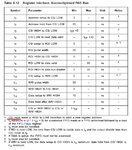
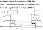
What follows are the Timing Table and the Timing Diagrams of my ASIC as per the datasheet:


The STM32F407 is running @ 168 Mhz, so a clock cycle = 5.95nS. According to the datasheet of my ASIC, "CS/ must make a HIGH to LOW transition to latch a new register address. That is t3 in the Timing Table. How the FSMC handles that?
Your help is highly appreciated..
- - - Updated - - -
Sorry, before I forgot to mention that the address signals A[3:0] are TTL-compatible inputs. As far as I know, some or most of the IOs on the STM32F4 are TTL tolerant, but does that presume ability in driving a TTL receiver? Do you think I need a logic/level translator on address, data, and other signals?
- - - Updated - - -
I just confirmed that I was able to write on the Command Register @ 0x03 and the interrupt that I got earlier was caused by an illegal command written to the Command Register. Also, I have been able to clear the interrupt by writing a software RESET command into the Command Register. However, reading other registers still gives incorrect data.
This is my first thread here, and I'm very glad to join your EE community.
Well, I have a problem getting the STM32F407 to talk with a legacy ASIC and I've been working very hard for the past two weeks trying to solve it. I will try to provide as much details as possible about the situation and my observations so far in order to make it much easier for you to help. Anyways, I would like to bring to your attention the fact that I did my homework in researching the problem very well, so be certain that this is not another "please-do-it-for-me" question!
Starting off with the ASIC being concerned, the chip provides an MPU interface ( PAD[7:0], CS, RD/, WR/, A[3:0] ) that can be used to access all internal registers in addition to another data-bus that can be used with an external DMA ( DB[7:0], DREQ, DACK, DBRD/, DBWR/ ) for transfer of data between the ASIC and the host uC. The PAD[7:0] bus may be used as a data-only bus in the nonmultiplexed mode, and a data/address bus in the multiplexed mode. Still not sure how both can be viewed/dealt with from the uC perspective.
For this purpose, I have designed a simple two-layer board that hosts the ASIC and all the other necessary components (20 MHz CMOS Crystal Circuit, GPIO headers for connection to uC, jumpers for modes, etc). Because the FSMC/FMC peripheral is the best bet to get things done easily for such a scenario, I have used it to connect to the ASIC and here is my CubeMx-Generated setup for FSMC:
Code:
FSMC_NORSRAM_TimingTypeDef Timing;


  /** Perform the NOR1 memory initialization sequence

  */

  hnor1.Instance = FSMC_NORSRAM_DEVICE;

  hnor1.Extended = FSMC_NORSRAM_EXTENDED_DEVICE;

  /* hnor1.Init */

  hnor1.Init.NSBank = FSMC_NORSRAM_BANK1;

  hnor1.Init.DataAddressMux = FSMC_DATA_ADDRESS_MUX_DISABLE; // This was not available within Cube.

  hnor1.Init.MemoryType = FSMC_MEMORY_TYPE_NOR; // >>>>>

  hnor1.Init.MemoryDataWidth = FSMC_NORSRAM_MEM_BUS_WIDTH_8;

  hnor1.Init.BurstAccessMode = FSMC_BURST_ACCESS_MODE_DISABLE;

  hnor1.Init.WaitSignalPolarity = FSMC_WAIT_SIGNAL_POLARITY_LOW;

  hnor1.Init.WrapMode = FSMC_WRAP_MODE_DISABLE;

  hnor1.Init.WaitSignalActive = FSMC_WAIT_TIMING_BEFORE_WS;

  hnor1.Init.WriteOperation = FSMC_WRITE_OPERATION_ENABLE;

  hnor1.Init.WaitSignal = FSMC_WAIT_SIGNAL_DISABLE;

  hnor1.Init.ExtendedMode = FSMC_EXTENDED_MODE_DISABLE; // >>>>>>

  hnor1.Init.AsynchronousWait = FSMC_ASYNCHRONOUS_WAIT_DISABLE;

  hnor1.Init.WriteBurst = FSMC_WRITE_BURST_DISABLE;

  hnor1.Init.PageSize = FSMC_PAGE_SIZE_NONE;

  /* Timing */

  Timing.AddressSetupTime = 0;

  Timing.AddressHoldTime = 3;

  Timing.DataSetupTime = 5;

  Timing.BusTurnAroundDuration = 0;

  Timing.CLKDivision = 0; // >>>>>

  Timing.DataLatency = 0; // >>>>>

  Timing.AccessMode = FSMC_ACCESS_MODE_A;

  /* ExtTiming */


  if (HAL_NOR_Init(&hnor1, &Timing, NULL) != HAL_OK)

  {

    Error_Handler();

  }
Write/Read accesses are done as follows:
Code:
#define ASIC_ADDR    ((uint32_t)0x60000000)


uint8_t ASIC_ReadReg()

{

 return *(uint8_t*)ASIC_ADDR;

}


void ASIC_WriteReg(uint8_t RegValue)

{

 *(uint8_t*)ASIC_ADDR = RegValue;

}
The ASIC doesn't have any means for debugging or verifiying functionality, so the only viable way for me to check it was by performing hundreds of write/read trials under dozens of different hardware/software configurations and observing the outcome. I was initially writing an 8-bit buffer (0xAA) followed by a number of successive reads. The value returned by the ASIC_ReadReg() function was the same value I wrote earlier, 0xAA. To make sure the program doesn't read a circular buffer or FIFO of the STM32F4 uC itself, I removed the power line for the ASIC board several times during the reading loop, which has resulted in a 0x00 returned value.
Another trick was by performing a hardware RESET (asserting RESET signal for 10uS) to check whether the chip is responding, and that has resulted in a 0x00 returned value, as well, which means the chip has been reset and the buffer I was reading has been cleared, as well!
After hundreds of tests playing with several pins, enabling/disabling pull-ups/downs on certain signals, modifying timings for FSMC, I managed to detect an interrupt fired when I write any non-zero value into the ASIC. I noticed that the interrupt will not fire again unless the ASIC was reset, which means the INT flag has been cleared and the chip is ready to respond for a new interrupt.
Last results obtained by changing the address to the following:
Code:
#define ASIC_ADDR ((uint32_t*)0x60000000) // Casting to Pointer
Code:
RD_Val = *(uint8_t*)*ASIC_ADDR; // Reading a pointer?Still not sure what part of the chip I was reading, and how to target/address a certain register. From my experience interfacing an LCD in similar fashion (8080 interface), the RS signal was used to select between registers and data ram. In the nonmultiplexed mode, the A[3:0] signals are used to select registers, but I don't seem to get the expected values according to the datasheet.
What follows are the Timing Table and the Timing Diagrams of my ASIC as per the datasheet:


The STM32F407 is running @ 168 Mhz, so a clock cycle = 5.95nS. According to the datasheet of my ASIC, "CS/ must make a HIGH to LOW transition to latch a new register address. That is t3 in the Timing Table. How the FSMC handles that?
Your help is highly appreciated..
- - - Updated - - -
Sorry, before I forgot to mention that the address signals A[3:0] are TTL-compatible inputs. As far as I know, some or most of the IOs on the STM32F4 are TTL tolerant, but does that presume ability in driving a TTL receiver? Do you think I need a logic/level translator on address, data, and other signals?
- - - Updated - - -
I just confirmed that I was able to write on the Command Register @ 0x03 and the interrupt that I got earlier was caused by an illegal command written to the Command Register. Also, I have been able to clear the interrupt by writing a software RESET command into the Command Register. However, reading other registers still gives incorrect data.
Last edited: