Continue to Site

Welcome to EDAboard.com

Welcome to our site! EDAboard.com is an international Electronics Discussion Forum focused on EDA software, circuits, schematics, books, theory, papers, asic, pld, 8051, DSP, Network, RF, Analog Design, PCB, Service Manuals... and a whole lot more! To participate you need to register. Registration is free. Click here to register now.

S21 response on CMOS Power Amplifier

Status
Not open for further replies.

Fhasan

Newbie level 6
Joined
Oct 3, 2010
Messages
13
Helped
0
Reputation
0
Reaction score
0
Trophy points
1,281
Activity points
1,377
Hi all,

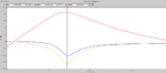
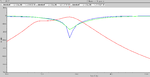
Currently i'm designing CMOS PA in cadence tool, my PA response are listed below:

1. S11 at 27Ghz is -17.311 db
2. S22 at 27 Ghz is -15.23 db
3. Unfortunately my S21 response is below 0 db (-19.44db).

I have go thru others researches paper their response for S21 is above 10db. I'm using cascade topology and even after increasing the stage I still couldn't get better S21 response.:-( Any idea how to get better S21 response?

p/s: I did design for 2.4Ghz, and manage to get S21 above 0 db.
 

Are you talking about simulation or hardware measurement? In the former case, trace the input signal through the amplifier and check against expected signal level in each stage.
 
  • Like
Reactions: Fhasan

    Fhasan

    Points: 2
    Helpful Answer Positive Rating
Are you talking about simulation or hardware measurement? In the former case, trace the input signal through the amplifier and check against expected signal level in each stage.

Thanks for ur reply. I'm talking about simulation. Attached here is two files on S-parameter responses for 2.4GHz and 28GHz.

- - - Updated - - -

Thanks for ur reply. I'm talking about simulation. Attached here is two files on S-parameter responses for 2.4GHz and 28GHz.

Reattached the files
 

Attachments

  • 2.4GHz Response.png
    2.4GHz Response.png
    21.7 KB · Views: 104
  • 28GHz Response.png
    28GHz Response.png
    21.3 KB · Views: 107
  • 28GHz Response.png
    28GHz Response.png
    21.3 KB · Views: 113
  • 2.4GHz Response.png
    2.4GHz Response.png
    21.7 KB · Views: 93

Post your schematic.. Give the details about the PDK which you work with.
 

As said, it's easy to find out in simulation why there's no or insufficient gain.
 

Attached is the Schematic design picture together with S parameter response. I'm using 0.18um process technology.

Schematic Design.png28GHz Response.png2.4GHz Response.png
 

Is 0.18um process suitable for 28Ghz amplification ?? I don't think so..
What about the fT of the MOS ?? It should be more than 100GHz for a appropriate operation.
We don't know DC bias points too and Inductor/Capacitor values..
It's really hard to say something.
 
  • Like
Reactions: FvM

    FvM

    Points: 2
    Helpful Answer Positive Rating
Agreed, the technology is likely the issue. Have you seen any examples of other using this process for >27GHz?

Perhaps if you try using ideal inductors instead of the PDK ones it will work better... but only in simulation.
 

Yes i have seen other researches manage to get good response on 0.18um for >27GHz. One of the example can be found in the paper entitle "A Ka-Band CMOS Low-Noise Amplifier for
Ka-Band Communication System" written in 2010 by Zhe Yang Huang.
Agreed, the technology is likely the issue. Have you seen any examples of other using this process for >27GHz?

Perhaps if you try using ideal inductors instead of the PDK ones it will work better... but only in simulation.
 

Yes i have seen other researches manage to get good response on 0.18um for >27GHz. One of the example can be found in the paper entitle "A Ka-Band CMOS Low-Noise Amplifier forKa-Band Communication System" written in 2010 by Zhe Yang Huang.
But which 0.18um process ?? Every Foundry may have a 0.18um process but it doesn't mean that each one would be used for mmWave application.
That's the point which you confuse..
 

Status
Not open for further replies.

Part and Inventory Search

Welcome to EDABoard.com

Sponsor

Back
Top