Continue to Site

Welcome to EDAboard.com

Welcome to our site! EDAboard.com is an international Electronics Discussion Forum focused on EDA software, circuits, schematics, books, theory, papers, asic, pld, 8051, DSP, Network, RF, Analog Design, PCB, Service Manuals... and a whole lot more! To participate you need to register. Registration is free. Click here to register now.

Fast switching transistor with slow rise/fall times, why?

Status
Not open for further replies.

righteous

Full Member level 2
Joined
Nov 29, 2017
Messages
130
Helped
0
Reputation
0
Reaction score
0
Trophy points
16
Activity points
1,282
Gentlemen,

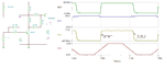
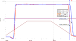
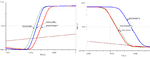
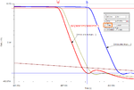
It is my objective to put as much current in the least amount of time possible through R5. However I'm experiencing rise and fall times of Q2 are anything but appropriate for a transistor like Q2, and due to my limited experience with analog design I'm finding it difficult to debug.

Here is my circuit, and DC calculations are courtesy of partsim.com:
Screenshot from 2017-11-29 14-54-13.png

The V1 period is 100uS and pulse is 50ns rise, 50ns width, 50ns fall, Here is the simulated transient analysis where ORANGE is left side of R4, and RED is base of Q2, and BLUE is collector of Q2:
Screenshot from 2017-11-29 14-03-19.png

Any ideas/suggestion are highly welcome.
 

This is an almost impossible "mission", the input pulse is too short.
And ..you know the usual rule:
the transistor (used as a fast switch) should not be driven into the saturation range ...
 
This is an almost impossible "mission", the input pulse is too short.

Sorry for my confusion, what do you mean by "too short"? If you mean it's too short for my specific circuit, I'm more than happy to look into an other solution.

And ..you know the usual rule:
the transistor (used as a fast switch) should not be driven into the saturation range ...

I guess someone told me that 30 years ago, but I had happily forgotten it. Thank you for the reminder ;-)
 

The slow rise time is observed due to unsuitable circuit, the fall time doesn't look bad for the used transistors, I think.
 

A speed up capacitor at the base of both transistors will certainly help.
 

How you have no current passing through R3. If you check, your voltage drop on R3 is 0 !!

There should a problem here. Check the current for your transistors, they seem to be off !
 

The circuit annotation is partly confusing, but I see a 0.7 V R3 voltage drop indicated. That's apparently too low to turn Q3 on fast enough.

Q3 is finally even saturated (Vce < Vbe), but it takes 200 ns. There are two options
- staying with saturated switching, speeding it up by appropriate means
- redesign the circuit for non-saturated switching, accepting higher voltage drops and power dissipation
 

Here is a switching circuit that may meet your specifications. It has some speed-up elements to enable fast switching. It uses commonly available transistors. I can't guarantee how it will perform with the transistors in your circuit. Not bench tested!
 

Attachments

  • fast_sw.png
    fast_sw.png
    31.1 KB · Views: 313
  • Like
Reactions: FvM

    FvM

    Points: 2
    Helpful Answer Positive Rating
Gents,

I would like to thank everyone for their valuable input so far. I was suggested to me to insert a push/pull pair of transistors between the two existing transistors, as the slow rise/fall times could be attributed to capacitance of the junctions. Here is the revised circuit and transient analysis. Now I have to build and test it.
Screenshot from 2017-11-30 10-33-47.png

Screenshot from 2017-11-29 17-43-52.png
 

Here is a switching circuit that may meet your specifications. It has some speed-up elements to enable fast switching. It uses commonly available transistors. I can't guarantee how it will perform with the transistors in your circuit. Not bench tested!

Dear Mr. E-design,

Thank you for valuable proposal, the LC looks interesting (black magic) to me, I will definitely give it a try and let you know.
 

@post #8: The 470 nH is the parasitic ESL of the cap ? Because if not, I do not see its need.
Using C2=100 pF and no inductance switches faster than 68 pF + 470 nH inductance. Not a lot faster, but faster.

Used Tina TI 9, measured from ~0 V to 10 V, the rise time gives this:
68pF + 470 nH --> tr=4.67 ns
100pF with no inductance --> tr=4 ns
 

@post #8: The 470 nH is the parasitic ESL of the cap ? Because if not, I do not see its need.
Using C2=100 pF and no inductance switches faster than 68 pF + 470 nH inductance. Not a lot faster, but faster.

You are correct, but adding the inductor was for a reason. I wasn't happy with the pulse-width error that was present using only a capacitor to aid with speed-up. It can be seen on the plot it reduces the overall width error by about 1.5nS on the rising edge and 4.4nS on the falling edge. So, this combination gave me the best switching speed with the least amount of pulse-width error. It may be an overkill for this specific application.

- - - Updated - - -

Using a 2N3904 and 2N3906 instead, seems to give even better speeds, resulting in tr ~ 4nS and tf ~ 3nS.
 

Attachments

  • fast_sw_width.png
    fast_sw_width.png
    50.2 KB · Views: 223
  • fast_sw_delay.png
    fast_sw_delay.png
    42.4 KB · Views: 204
  • faster.png
    faster.png
    42.3 KB · Views: 338
  • Like
Reactions: CataM

    CataM

    Points: 2
    Helpful Answer Positive Rating
Obviously using a medium current transistor with respective higher capacitances and lower ft has some impact on the switching speed. Question is why you are using it and presumed there's a reason, is the performance loss still acceptable?
 

Obviously using a medium current transistor with respective higher capacitances and lower ft has some impact on the switching speed. Question is why you are using it and presumed there's a reason, is the performance loss still acceptable?

The reason for using it requires a long explanation that is obsolete, so let's say I'm urinating with the equipment at hand (pun intended), but subsequently I sold my soul to Farnell, so if there are better options I'm all ears.
 

Keep us posted on the results, since I have some doubts about the performance of your circuit.

I built it, and you are right, it performs nothing like the sim, it sux. For starters I can't get Q1 to open unless I change R1 to 22R, and R3 to 470R, and so on... nothing get through to Q2. Not worth the time. I'll try your proposal now.

- - - Updated - - -

Here is a switching circuit that may meet your specifications. It has some speed-up elements to enable fast switching. It uses commonly available transistors. I can't guarantee how it will perform with the transistors in your circuit. Not bench tested!

I recreated your circuit in partsim.com, it didn't look exactly like your sim, so I tweaked it a bit and changed R6 to 220R and C2 to 47pF, then it looks more like your sim and I even managed to shave ~20ns off the pulse width. Now I have to see what I can do about sourcing some suitable transistors and build it.
Screenshot from 2017-12-01 13-36-17.png

- - - Updated - - -

update for #17

As you proposed, Using a 2N3904 and 2N3906 instead, seems to shave another ~20ns of the pulse width too.
Screenshot from 2017-12-01 14-20-06.png

Now my concern is that 2N3906 can't handle the currents that I have planned for next iteration, and which was a reason to use NSS40300MZ4. I would like that T2 could handle 2> amps during 'on' period, could you possible suggest a suitable candidate? Or could I use two (or more) 2N3906 in 'parallel' like below, or does that constitute an electronic faux pas? (I'm asking out of ignorance)
Screenshot from 2017-12-01 14-41-00.png
 

I recreated your circuit in partsim.com, it didn't look exactly like your sim, so I tweaked it a bit and changed R6 to 220R and C2 to 47pF, then it looks more like your sim and I even managed to shave ~20ns off the pulse width.
R6 has next to nothing of a role in the switching characteristic. 220 ohms gives around 3mA of quiescent current.. a bit too much for a pull down resistor.

Now my concern is that 2N3906 can't handle the currents that I have planned for next iteration, and which was a reason to use NSS40300MZ4. I would like that T2 could handle 2> amps during 'on' period, could you possible suggest a suitable candidate?
The bipolar technology is not very suitable for high speed and high power applications. As it was already mentioned, as you go up in power, the capacitances and transition frequency increase and decrease respectively, affecting the switching performance.

Or could I use two (or more) 2N3906 in 'parallel' like below, or does that constitute an electronic faux pas? (I'm asking out of ignorance)
The negative temperature coefficient of the PNP BJT transistor makes it unsuitable for parallelizing unless additional protective means is implemented e.g. negative feedback via a resistor in the collector of each transistor.
In other words, as the temperature of the transistor goes up, the emitter-collector drop goes down, making one single transistor to hog all the current leaving the others with nothing.
 

R6 has next to nothing of a role in the switching characteristic. 220 ohms gives around 3mA of quiescent current.. a bit too much for a pull down resistor.

Noted.

The bipolar technology is not very suitable for high speed and high power applications. As it was already mentioned, as you go up in power, the capacitances and transition frequency increase and decrease respectively, affecting the switching performance.

Ok then I'll bite the bullet and continue with BJT and accept some minor decrease in switching performance. FET's don't seem to be able to do what I want, as I would need one without built-in fly-back diode and a RDS(on) < 1Ω at the operating voltages indicated. Below is what I came up with, fiddling around with Mr. E-design's proposal.

But now I'm concerned about the relative excessive current going through R3, can it be improved without affecting the switching further?

At the same time I note that base of Q1 (black) goes negative in the sim, would that indicate that the circuit would not work as sim'ed? Or is there another reason for the negative peak?

Screenshot from 2017-12-01 17-30-35.pngScreenshot from 2017-12-01 17-29-41.png


The negative temperature coefficient of the PNP BJT transistor makes it unsuitable for parallelizing unless additional protective means is implemented e.g. negative feedback via a resistor in the collector of each transistor. In other words, as the temperature of the transistor goes up, the emitter-collector drop goes down, making one single transistor to hog all the current leaving the others with nothing.

Noted, I recall now hearing something along those lines in my earlier days.
 

At the same time I note that base of Q1 (black) goes negative in the sim, would that indicate that the circuit would not work as sim'ed? Or is there another reason for the negative peak?
No. The negative current means that it is pulling out charge from the base, turning it off faster. The peak negative current is higher with respect to the current you would notice if there was no speed-up capacitor at the base. You need to remove the charge from the base emitter junction before the current goes to 0, just like the reverse recovery of a diode.
 

Status
Not open for further replies.

Similar threads

Part and Inventory Search

Welcome to EDABoard.com

Sponsor

Back
Top